|
전자부품 데이터시트 검색엔진 |
|
|
전자부품 데이터시트 검색엔진 |
|
AS7225 데이터시트(PDF) 67 Page - OSRAM GmbH |
|
|
|||||||||||||||||||||||||||||
AS7225 데이터시트(HTML) 67 Page - OSRAM GmbH |
|
|
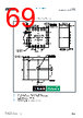
67 / 76 page  Document Feedback AS7225 Application Information Datasheet • PUBLIC DS000496 • v2-00 • 2019-Jun-28 75 │ 66 13.3 PCB Pad Layout Suggested PCB pad layout guidelines for the LGA package are shown. Flash Gold is recommended as a surface finish for the landing pads. Figure 90: Recommended PCB Pad Layout (Top View) (1) Unless otherwise specified, all dimensions are in millimeters. (2) Add 0.05 mm all around the nominal lead width and length for the PCB pad land pattern. (3) This drawing is subject to change without notice. |
|
링크 URL |
| ALLDATASHEET 가 귀하에 도움이 되셨나요? [ DONATE ] |
Alldatasheet는? | 광고문의 | 운영자에게 연락하기 | 개인정보취급방침 | 링크 투 데이터시트 | 링크교환 | 제조사별 검색 All Rights Reserved©Alldatasheet.com |
| Russian : Alldatasheetru.com | Korean : Alldatasheet.co.kr | Spanish : Alldatasheet.es | French : Alldatasheet.fr | Italian : Alldatasheetit.com Portuguese : Alldatasheetpt.com | Polish : Alldatasheet.pl | Vietnamese : Alldatasheet.vn Indian : Alldatasheet.in | Mexican : Alldatasheet.com.mx | British : Alldatasheet.co.uk | New Zealand : Alldatasheet.co.nz |
|
Family Site : ic2ic.com |
icmetro.com |
 Korean ▼
 English
 Chinese
 German
 Japanese
 Russian
 Korean
 Spanish
 French
 Italian
 Portuguese
 Polish
 Vietnamese
 Indian
 Mexican
 British
 New Zealand