|
전자부품 데이터시트 검색엔진 |
|
|
전자부품 데이터시트 검색엔진 |
|
SA5753 데이터시트(PDF) 6 Page - NXP Semiconductors |
|
|
|||||||||||||||||||||||||||||
SA5753 데이터시트(HTML) 6 Page - NXP Semiconductors |
|
|
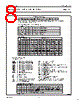
6 / 15 page  Philips Semiconductors Product specification SA5753 Audio processor – filter and control section 1997 Nov 07 6 e. A4 compensates for transmit gain variations due to manufacturing tolerances of the SA5753, SA5752 and VCO connected to TXOUT (Pin 20). After A2a has been adjusted to set dynamic range then A4 is used to set the peak output voltage at TXOUT (Pin 20) such that a nominal 10kHz/V VCO produces a peak deviation of 12kHz to meet AMPS specifications. f. A6 is the volume control for both the SPKROUT and EAROUT. g. A7 compensates for manufacturing tolerances in the SA5753 and preceeding demodulator. For AMPS requirements, a 1kHz tone with 2.9kHz deviation should produce an output signal at DEMPOUT (Pin 7) corresponding to the zero crossing signal level of the expandor. NAMPS and VCO Offsets For NAMPS applications, a ‘1’ programmed into R5B3 (register 5, bit 3) will offset the transmit gain for NAMPS applications. It is recommended that A2a and A4 be programmed after the NAMPS option is set to compensate for manufacturing tolerances in the NAMPS offset, itself. When the VCO bit of R5B2 is a ‘1’, an extra gain of 6dB is provided at TXOUT for direct interface to VCOs with a nominal gain of 5kHz/V. Operation Using the I2C Communications Bus The SA5753 includes on-chip gain blocks and options which can be programmed through an I2C interface bus. To use this capability, the DFT pin (Pin 13) must be pulled LOW. In this mode, all signal level adjustments can be made through software with no external potentiometers required. With DFT pulled LOW, the HPDN pin (Pin 6) is an OUTPUT having the same value as the program bit in register 5 bit 1 (R5B1) of the control register bit map. The value at the VOXCTL output (Pin 5) is the same as the program bit in R8B7. The HPDN and VOXCTL outputs can be used to control the state of the SA5752 companion device. Power On Reset and Power Down Modes In order to avoid undefined states of the SA5753 when power is initially applied, a power-on-reset circuit is incorporated which defaults RxP and TxP such that the receive and transmit paths are muted if a ‘high’ voltage is applied to RX MUTE and TX MUTE (Pins 12 and 18). RX MUTE and TX MUTE include on-chip pull up resistors so, during power up, the user may apply a logic ‘1’ to these pins or leave them floating. After power up, the registers can be programmed and the mutes removed by a quick access write to R0. Three software controlled low power modes are provided on the SA5753. These are POWER DOWN (PWDN), IDLE and DENA and can be selected by programming a ‘1’ into R6B2, R6B1 or R6B0 as follows. In PWDN mode (R6B2=1) both the voice and data channels are powered down with the respective I/O pins at a high impedance. In DENA mode (R6B1=1) the voice channels are powered down, but the data channel (from DATAIN and TXOUT) is fully active. In IDLE mode (R6B1=1, R6B0=1) both voice and data channels are powered down. (See Table on page 8.) The difference between selecting IDLE and PWDN is that the former maintains the normal operational bias voltages at all voice and data I/O pins and provides a glitch-free transfer from power down to a fully active mode and vice-versa. Although the POWER DOWN mode exhibits lower power consumption, glitches may occur when transferring to an active mode because of the previous high impedance of the I/O pins. The VOXCTL and HPDN pins (Pins 5 and 6) still have the same value as R8B7 and R5B1 in all low power modes. Operation Without Using the I2C Bus The SA5753 can be operated in a default mode with the I2C bus bypassed. To use this mode, the DFT pin (Pin 13) is pulled HIGH, then the I2C bus is bypassed and the SA5753 operates as if all register bits in the I2C address map table are set to ‘0’ except R1B2 (S13), R0B0 (S10) and R0B1 (S9), which are set to ‘1’ to enable the receiver output. R6B2 (PWDN), which is controlled by the state of the HPDN pin (Pin 6), which is an input in DEFAULT mode. When HPDN is pulled HIGH, the R6B2 bit is set to ‘0’ and the SA5753 is placed in it’s normal operating mode with all Gain Control Blocks set to 0dB except A3, which is set to –2dB. When HPDN is pulled LOW, the R6B2 bit is set to ‘1’ and the SA5753 enters POWER DOWN. There is no on-chip pull-up or pull-down structure on the HPDN pin and so it must not be allowed to float in DEFAULT mode since the operating mode of the SA5753 will then be undetermined. The Tx MUTE and Rx MUTE pins must be pulled LOW to enable the transmit and receive paths, respectively. The VOXCTL pin (Pin 5) will follow the value of the control bit stored in R8B7 prior to pulling DFT HIGH. The DTMF is disabled in the DEFAULT mode. Programming Without the I2C Protocol In the default mode, with DFT (Pin 13) and HPDN (Pin 6) pulled HIGH, the registers in the control register bit map are chained together so that bit 0 of a register is connected to bit 7 of the preceeding register with R0B6, R0B7, R1B6 and R1B7 bypassed, i.e., R0B5 is connected to R1B0, R1B5 is connected to R2B0, R2B7 is connected to R3B0, etc. Bits can then be loaded as a serial stream through the SDA pin of the I2C bus by the negative edge of a shifting clock applied at the SCL pin of the I2C bus. When a bit is loaded at SDA it will load first into R0B0 and then will be shifted to R8B7 after 68 clock edges. A total of 68 clock pulses (applied at SCL) are therefore required to completely load the registers. In this mode of operation the contents of the register map are also shifted out from the VOXCTL pin since it takes the same value as R8B7. After power up there is no reset within the registers so the first 68 bits clock out at the VOXCTL pin will have an indeterminate value. Summary: To use this capability, the DFT pin and the HPDN pin must be pulled HIGH, the serial bit stream loaded through SCL synchronous with the negative clock edge applied at SCL for 68 clock pulses, and then the DFT pin pulled LOW. NOTE: Default Mode is not tested in production. |
|
|
링크 URL |
| ALLDATASHEET 가 귀하에 도움이 되셨나요? [ DONATE ] |
Alldatasheet는? | 광고문의 | 운영자에게 연락하기 | 개인정보취급방침 | 링크 투 데이터시트 | 링크교환 | 제조사별 검색 All Rights Reserved©Alldatasheet.com |
| Russian : Alldatasheetru.com | Korean : Alldatasheet.co.kr | Spanish : Alldatasheet.es | French : Alldatasheet.fr | Italian : Alldatasheetit.com Portuguese : Alldatasheetpt.com | Polish : Alldatasheet.pl | Vietnamese : Alldatasheet.vn Indian : Alldatasheet.in | Mexican : Alldatasheet.com.mx | British : Alldatasheet.co.uk | New Zealand : Alldatasheet.co.nz |
|
Family Site : ic2ic.com |
icmetro.com |
 Korean ▼
 English
 Chinese
 German
 Japanese
 Russian
 Korean
 Spanish
 French
 Italian
 Portuguese
 Polish
 Vietnamese
 Indian
 Mexican
 British
 New Zealand