|
전자부품 데이터시트 검색엔진 |
|
|
전자부품 데이터시트 검색엔진 |
|
SA5753 데이터시트(PDF) 7 Page - NXP Semiconductors |
|
|
|||||||||||||||||||||||||||||
SA5753 데이터시트(HTML) 7 Page - NXP Semiconductors |
|
|
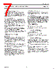
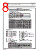
7 / 15 page  Philips Semiconductors Product specification SA5753 Audio processor – filter and control section 1997 Nov 07 7 Cordless Telephone Applications For cordless telephone applications, a switch S12 is provided (R5B0) to route data through the complete transmit path while inhibiting the voice channel. In the receive path, a quick access mode is provided through the I2C to disable both EAROUT and SPKROUT, by setting R0B0 and R0B1, when data is detected at the DEMPOUT pin (Pin 7). I2C CHARACTERISTICS The I2C bus is for 2-way, 2-line communication between different ICs or modules. The two lines are a serial data line (SDA) and a serial clock line (SCL). Both SDA and SCL are bidirectional lines connected to a positive supply voltage via a pull-up resistor. When the bus is free, both lines are HIGH. Data transfer may be initiated only when the bus is not busy (both lines HIGH). The output devices, or stages, connected to the bus must have an open drain or open collector output in order to perform the wired-AND function. Data at the I2C bus can be transferred at a rate up to 100kbits/s. The number of devices connected to the bus is solely dependent on the maximum allowed bus capacitance of 400pF. For devices operating over a wide range of supply voltages, such as the SA5753, the following levels have been defined for a logical LOW and HIGH; VILMAX = 0.3VDD (max. input LOW voltage) VIHMIN = 0.7VDD (min. input HIGH voltage) Data Transfer Data is transferred from a transmitting device to a receiving device with one data bit transferred during each clock pulse on the SCL line. The transmitter also generates the clock once arbitration has given it control of the SCL line. The data on the SDA line must remain stable during the HIGH period of the clock cycle, otherwise it may be interpreted as a control signal. Start and Stop Conditions Both data and clock lines remain HIGH when the bus is not busy. A HIGH to LOW transition of the data line while the clock line is HIGH is defined as a start condition. A LOW to HIGH transition of the data line while the clock is HIGH is defined as a stop condition. Acknowledgement Following each byte of data transfered, the receiver must acknowledge successful reception. To do this the transmitter releases the SDA line (allowing it to go HIGH) at the end of each transmitted byte, and it is pulled LOW by the receiver. If this condition is maintained during the next HIGH period of the clock pulse (called the acknowledge clock pulse) then data transfer is resumed. If the receiver does not pull the SDA line LOW, the transmitter will abort the transfer. I2C Bus Data Configurations The SA5753 is always a slave receiver in the I2C bus configuration). The slave address consists of eight bits in the serial mode and is internally fixed. Control Registers The control register bit map is shown below. Either a quick access or normal address mode can be used, determined by the two MSB bits in the first word following the SA5753 address word. If the quick access mode is used, the registers R0 or R1 can be updated by sending only two bytes of information (address plus update). If R0 or R1 are updated using the address mode, then B7 and B6 of the data word are ignored. In all access modes, incremental register addressing is supported with following words updating the next register until a ‘stop’ bit is sent. High Tone DTMF Register MSB LSB HD7 HD6 HD5 HD4 HD3 HD2 HD1 HD0 The eight bits determine the output frequency by the following formula.: High Frequency = 1200kHz/6/HD where HD is the value of the register. Low Tone DTMF Register MSB LSB LD7 LD6 LD5 LD4 LD3 LD2 LD1 LD0 The eight bits determine the output frequency by the following formula.: Low Frequency = 1200kHz/14/LD where LD is the value of the register. The operation of the 96ms DTMF timer is initiated by the loading of the low tone DTMF register. This timer terminates transmission of the tones as the generated tones cross the reference level after 96ms. The on time of the tones can thus vary by up to one cycle of the tones. Continuous tones can be obtained by again loading DTC = 1 in R1, bit 5. Single tones can be obtained by loading 2 into the unused tone register to silence it. Loading a value of 1 or 0 into the registers will default the register value to 257 or 256 for high tone or low tone, respectively. Phase continuous frequency modulation can be produced by loading a new value into a DTMF register during continuous operation (DTC=1). |
|
|
링크 URL |
| ALLDATASHEET 가 귀하에 도움이 되셨나요? [ DONATE ] |
Alldatasheet는? | 광고문의 | 운영자에게 연락하기 | 개인정보취급방침 | 링크 투 데이터시트 | 링크교환 | 제조사별 검색 All Rights Reserved©Alldatasheet.com |
| Russian : Alldatasheetru.com | Korean : Alldatasheet.co.kr | Spanish : Alldatasheet.es | French : Alldatasheet.fr | Italian : Alldatasheetit.com Portuguese : Alldatasheetpt.com | Polish : Alldatasheet.pl | Vietnamese : Alldatasheet.vn Indian : Alldatasheet.in | Mexican : Alldatasheet.com.mx | British : Alldatasheet.co.uk | New Zealand : Alldatasheet.co.nz |
|
Family Site : ic2ic.com |
icmetro.com |
 Korean ▼
 English
 Chinese
 German
 Japanese
 Russian
 Korean
 Spanish
 French
 Italian
 Portuguese
 Polish
 Vietnamese
 Indian
 Mexican
 British
 New Zealand