|
전자부품 데이터시트 검색엔진 |
|
|
전자부품 데이터시트 검색엔진 |
|
AK6510C 데이터시트(PDF) 5 Page - Asahi Kasei Microsystems |
|
|
|||||||||||||||||||||||||||||
AK6510C 데이터시트(HTML) 5 Page - Asahi Kasei Microsystems |
|
|
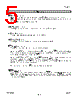
5 / 18 page  ASAHI KASEI [AK6514C] DAP04E-00 2005/03 - 5 - Pin Description CS (Chip Select Input) When CS changes high level to low level, the AK6514C can receive the instructions. CS should be kept low level while receiving op-code, address and data, and while outputting data. When CS is high level, SO indicate Hi-Z. SCK (Serial Clock Input) The SCK clock pin is the synchronous clock input for input/output data. SI (Serial Data Input) The op-code, address, and data are written to the SI pin. SO (Serial Data Output) The SO pin outputs the data from memory array and status register. WP (Write Protect Input) The WP pin controls the write function to the status register. When the WPEN bit in the status register is "0", the function of WP pin becomes disable. Then the status register can be programmable when the WEN bit in the status register is "1". And it does not depend on the status of WP pin. When the WPEN bit is "1", the function of WP is enabled. Then the status register can not be programmable when the WEN bit is "1" and the status of WP pin is low. When the WPEN bit is "1", WP pin is high and WEN bit is "1", AK6514C can accept the WRITE instruction to the status registers. During the instruction input, WP pin should keep high or low level. HOLD (Hold Input) The HOLD pin can hold the data transfer. When the HOLD pin changes hi to low while the SCK is low, the data transfer is held. And the transfer starts when the HOLD pin changes low to high while the SCK is low. While the holding the data transfer, AK6514C ignores the clock signal on SCK pin. |
|
|
링크 URL |
| ALLDATASHEET 가 귀하에 도움이 되셨나요? [ DONATE ] |
Alldatasheet는? | 광고문의 | 운영자에게 연락하기 | 개인정보취급방침 | 링크 투 데이터시트 | 링크교환 | 제조사별 검색 All Rights Reserved©Alldatasheet.com |
| Russian : Alldatasheetru.com | Korean : Alldatasheet.co.kr | Spanish : Alldatasheet.es | French : Alldatasheet.fr | Italian : Alldatasheetit.com Portuguese : Alldatasheetpt.com | Polish : Alldatasheet.pl | Vietnamese : Alldatasheet.vn Indian : Alldatasheet.in | Mexican : Alldatasheet.com.mx | British : Alldatasheet.co.uk | New Zealand : Alldatasheet.co.nz |
|
Family Site : ic2ic.com |
icmetro.com |
 Korean ▼
 English
 Chinese
 German
 Japanese
 Russian
 Korean
 Spanish
 French
 Italian
 Portuguese
 Polish
 Vietnamese
 Indian
 Mexican
 British
 New Zealand