|
전자부품 데이터시트 검색엔진 |
|
|
전자부품 데이터시트 검색엔진 |
|
PL611S-19-XXXTC-R 데이터시트(PDF) 6 Page - PhaseLink Corporation |
|
|
|||||||||||||||||||||||||||||
PL611S-19-XXXTC-R 데이터시트(HTML) 6 Page - PhaseLink Corporation |
|
|
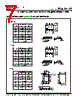
6 / 8 page  (Preliminary)PL611s-19 0.5kHz-55MHz MHz to KHz Programmable Clock TM 47745 Fremont Blvd., Fremont, California 94538 Tel (510) 492-0990 Fax (510) 492-0991 www.phaselink.com Rev 12/12/06 Page 6 PCB LAYOUT CONSIDERATIONS FOR PERFORMANCE OPTIMIZATION The following guidelines are to assist you with a performance optimized PCB design: - Keep all the PCB traces to PL611s-19 as short as possible, as well as keeping all other traces as far away from it as possible. - When a reference input clock is generated from a crystal, place the PL611s-19 ‘FIN’ as close as possible to the ‘Xout’ crystal pin. This will reduce the cross-talk between the reference input and the other signals. - Place a 0.01 F~0.1 F decoupling capacitor between VDD and GND, on the component side of the PCB, close to the VDD pin. It is not recommended to place this component on the backside of the PCB. Going through vias will reduce the signal integrity, causing additional jitter and phase noise. - It is highly recommended to keep the VDD and GND traces as short as possible. - When connecting long traces (> 1 inch) to a CMOS output, it is important to design the traces as a transmission line or ‘stripline’, to avoid reflections or ringing. In this case, the CMOS output needs to be matched to the trace impedance. Usually ‘striplines’ are designed for 50 impedance and CMOS outputs usually have lower than 50 impedance so matching can be achieved by adding a resistor in series with the CMOS output pin to the ‘stripline’ trace. - Please contact PhaseLink for the application note on how to design outputs driving long traces or for additional layout assistance. DFN-6L Evaluation Board |
|
|
링크 URL |
| ALLDATASHEET 가 귀하에 도움이 되셨나요? [ DONATE ] |
Alldatasheet는? | 광고문의 | 운영자에게 연락하기 | 개인정보취급방침 | 링크 투 데이터시트 | 링크교환 | 제조사별 검색 All Rights Reserved©Alldatasheet.com |
| Russian : Alldatasheetru.com | Korean : Alldatasheet.co.kr | Spanish : Alldatasheet.es | French : Alldatasheet.fr | Italian : Alldatasheetit.com Portuguese : Alldatasheetpt.com | Polish : Alldatasheet.pl | Vietnamese : Alldatasheet.vn Indian : Alldatasheet.in | Mexican : Alldatasheet.com.mx | British : Alldatasheet.co.uk | New Zealand : Alldatasheet.co.nz |
|
Family Site : ic2ic.com |
icmetro.com |
 Korean ▼
 English
 Chinese
 German
 Japanese
 Russian
 Korean
 Spanish
 French
 Italian
 Portuguese
 Polish
 Vietnamese
 Indian
 Mexican
 British
 New Zealand