|
전자부품 데이터시트 검색엔진 |
|
|
전자부품 데이터시트 검색엔진 |
|
RT8800AGQV 데이터시트(PDF) 2 Page - Richtek Technology Corporation |
|
|
|||||||||||||||||||||||||||||
RT8800AGQV 데이터시트(HTML) 2 Page - Richtek Technology Corporation |
|
|
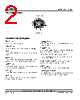
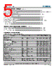
2 / 21 page  RT8800A 2 DS8800A-04 August 2007 www.richtek.com All brand name or trademark belong to their owner respectively Functional Pin Description IMAX (Pin 1) Over current protection setting. VID125 (Pin 2) Connect a resistor from this pin to GND can raise VOUT. FB (Pin 3) The pin is defined as the inverting input of internal error amplifier. DVD (Pin 4) The pin is defined as a programmable power UVLO detection input. Trip threshold = 0.8V at VDVD rising. COMP (Pin 5) The pin is defined as the output of the error amplifier and the input of all PWM comparators. PI (Pin 6) The pin is defined as the positive input of the error amplifier. RT (Pin 7) Switching frequency setting. Connect this pin to GND with a resistor to set the frequency. ICOMMON (Pin 8) Common negative input of current sense amplifiers for all three channels. PGOOD (Pin 9) Output power-good indication. The signal is implemented as an output signal with open-drain type. ISP1 , ISP2 , ISP3 (Pin 12, Pin 11, Pin 10) Current sense positive inputs for individual converter channel current sense. PWM1 , PWM2 , PWM3 (Pin 13, Pin 14, Pin 15) PWM outputs for each phase switching drive. VDD (Pin 16) Chip power supply. Connect this pin to a 5V supply. GND [Exposed Pad (17)] The exposed pad must be soldered to a large PCB and connected to GND for maximum power dissipation. Pin Configurations (TOP VIEW) VQFN-16L 3x3 IMAX ISP1 PGOOD ISP3 ISP2 DVD FB VID125 12 11 10 9 13 14 15 16 1 2 3 4 8 7 6 5 GND 17 |
|
|
링크 URL |
| ALLDATASHEET 가 귀하에 도움이 되셨나요? [ DONATE ] |
Alldatasheet는? | 광고문의 | 운영자에게 연락하기 | 개인정보취급방침 | 링크 투 데이터시트 | 링크교환 | 제조사별 검색 All Rights Reserved©Alldatasheet.com |
| Russian : Alldatasheetru.com | Korean : Alldatasheet.co.kr | Spanish : Alldatasheet.es | French : Alldatasheet.fr | Italian : Alldatasheetit.com Portuguese : Alldatasheetpt.com | Polish : Alldatasheet.pl | Vietnamese : Alldatasheet.vn Indian : Alldatasheet.in | Mexican : Alldatasheet.com.mx | British : Alldatasheet.co.uk | New Zealand : Alldatasheet.co.nz |
|
Family Site : ic2ic.com |
icmetro.com |
 Korean ▼
 English
 Chinese
 German
 Japanese
 Russian
 Korean
 Spanish
 French
 Italian
 Portuguese
 Polish
 Vietnamese
 Indian
 Mexican
 British
 New Zealand