|
전자부품 데이터시트 검색엔진 |
|
|
전자부품 데이터시트 검색엔진 |
|
FT201XS-R 데이터시트(PDF) 11 Page - Future Technology Devices International Ltd. |
|
|
|||||||||||||||||||||||||||||
FT201XS-R 데이터시트(HTML) 11 Page - Future Technology Devices International Ltd. |
|
|
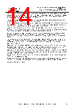
11 / 49 page  Copyright © 2014 Future Technology Devices International Limited 11 FT201X USB I2C SLAVE IC Datasheet Version 1.4 Document No.: FT_000627 Clearance No.: FTDI# 264 3.3 CBUS Signal Options The following options can be configured on the CBUS I/O pins. CBUS signal options are common to both package versions of the FT201X. These options can be configured in the internal MTP memory using the software utility FT_PROG, which can be downloaded from the FTDI Utilities (www.ftdichip.com). The default configuration is described in Section 9. CBUS Signal Option Available On CBUS Pin Description TRI-STATE CBUS0, CBUS1, CBUS2, CBUS3, CBUS4, CBUS5 IO Pad is tri-stated DRIVE 1 CBUS0, CBUS1, CBUS2, CBUS3, CBUS4, CBUS5 Output a constant 1 DRIVE 0 CBUS0, CBUS1, CBUS2, CBUS3, CBUS4, CBUS5 Output a constant 0 PWREN# CBUS0, CBUS1, CBUS2, CBUS3, CBUS4, CBUS5 Output is low after the device has been configured by USB, then high during USB suspend mode. This output can be used to control power to an external logic P-Channel logic level MOSFET switch. Enable the interface pull-down option when using the PWREN# in this way. SLEEP# CBUS0, CBUS1, CBUS2, CBUS3, CBUS4, CBUS5 Goes low during USB suspend mode. Typically used to power down an external logic. CLK24MHz CBUS0, CBUS1, CBUS2, CBUS3, CBUS4, CBUS5 24 MHz Clock output.* CLK12MHz CBUS0, CBUS1, CBUS2, CBUS3, CBUS4, CBUS5 12 MHz Clock output.* CLK6MHz CBUS0, CBUS1, CBUS2, CBUS3, CBUS4, CBUS5 6 MHz Clock output.* GPIO CBUS0, CBUS1, CBUS2, CBUS3, CBUS bit bang mode option. Allows up to 4 of the CBUS pins to be used as general purpose I/O. Configured individually for CBUS0, CBUS1, CBUS2 and CBUS3 in the internal MTP memory. A separate application note, AN232R-01, available from FTDI website (www.ftdichip.com) describes in more detail how to use CBUS bit bang mode. BCD Charger CBUS0, CBUS1, CBUS2, CBUS3, CBUS4, CBUS5 Battery charge Detect, indicates when the device is connected to a dedicated battery charger host. Active high output. BCD Charger# CBUS0, CBUS1, CBUS2, CBUS3, CBUS4, CBUS5 Inverse of BCD Charger (open drain) BitBang_WR# CBUS0, CBUS1, CBUS2, CBUS3, CBUS4, CBUS5 Synchronous and asynchronous bit bang mode WR# strobe output. BitBang_RD# CBUS0, CBUS1, CBUS2, CBUS3, CBUS4, CBUS5 Synchronous and asynchronous bit bang mode RD# strobe output. I2C_TXE# CBUS0, CBUS1, CBUS2, CBUS3, CBUS4, CBUS5 Transmit buffer empty, used to indicate to I2C master device status of the FT201EX transmit buffer I2C_RXF# CBUS0, CBUS1, CBUS2, CBUS3, CBUS4, CBUS5 Receive buffer full, used to indicate to I2C master device status of FT201EX receive buffer |
|
링크 URL |
| ALLDATASHEET 가 귀하에 도움이 되셨나요? [ DONATE ] |
Alldatasheet는? | 광고문의 | 운영자에게 연락하기 | 개인정보취급방침 | 링크 투 데이터시트 | 링크교환 | 제조사별 검색 All Rights Reserved©Alldatasheet.com |
| Russian : Alldatasheetru.com | Korean : Alldatasheet.co.kr | Spanish : Alldatasheet.es | French : Alldatasheet.fr | Italian : Alldatasheetit.com Portuguese : Alldatasheetpt.com | Polish : Alldatasheet.pl | Vietnamese : Alldatasheet.vn Indian : Alldatasheet.in | Mexican : Alldatasheet.com.mx | British : Alldatasheet.co.uk | New Zealand : Alldatasheet.co.nz |
|
Family Site : ic2ic.com |
icmetro.com |
 Korean ▼
 English
 Chinese
 German
 Japanese
 Russian
 Korean
 Spanish
 French
 Italian
 Portuguese
 Polish
 Vietnamese
 Indian
 Mexican
 British
 New Zealand