|
전자부품 데이터시트 검색엔진 |
|
|
전자부품 데이터시트 검색엔진 |
|
IS25LP016D-RMLA3 데이터시트(PDF) 50 Page - Integrated Silicon Solution, Inc |
|
|
|||||||||||||||||||||||||||||
IS25LP016D-RMLA3 데이터시트(HTML) 50 Page - Integrated Silicon Solution, Inc |
|
|
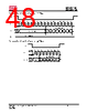
50 / 115 page  IS25LP016D IS25WP016D Integrated Silicon Solution, Inc.- www.issi.com 50 Rev. B16 01/01/2025 8.14 WRITE ENABLE OPERATION (WREN, 06h) The Write Enable (WREN) instruction is used to set the Write Enable Latch (WEL) bit. The WEL bit is reset to the write-protected state after power-up. The WEL bit must be write enabled before any write operation, including Sector Erase, Block Erase, Chip Erase, Page Program, Program Information Row, Write Status Register, Write Function Register, Set non-volatile Read Register, Set non-volatile Extended Read Register, and Write Autoboot Register operations except for Set volatile Read Register and Set volatile Extended Read Register. The WEL bit will be reset to the write-protected state automatically upon completion of a write operation. The WREN instruction is required before any above operation is executed. Figure 8.22 Write Enable Sequence In SPI Mode Instruction = 06h CE# SCK SI 0 1 2 3 4 5 6 7 Mode 3 Mode 0 SO High Impedance Figure 8.23 Write Enable Sequence In QPI Mode 06h CE# SCK IO[3:0] 0 1 Mode 3 Mode 0 |
|
링크 URL |
| ALLDATASHEET 가 귀하에 도움이 되셨나요? [ DONATE ] |
Alldatasheet는? | 광고문의 | 운영자에게 연락하기 | 개인정보취급방침 | 링크 투 데이터시트 | 링크교환 | 제조사별 검색 All Rights Reserved©Alldatasheet.com |
| Russian : Alldatasheetru.com | Korean : Alldatasheet.co.kr | Spanish : Alldatasheet.es | French : Alldatasheet.fr | Italian : Alldatasheetit.com Portuguese : Alldatasheetpt.com | Polish : Alldatasheet.pl | Vietnamese : Alldatasheet.vn Indian : Alldatasheet.in | Mexican : Alldatasheet.com.mx | British : Alldatasheet.co.uk | New Zealand : Alldatasheet.co.nz |
|
Family Site : ic2ic.com |
icmetro.com |
 Korean ▼
 English
 Chinese
 German
 Japanese
 Russian
 Korean
 Spanish
 French
 Italian
 Portuguese
 Polish
 Vietnamese
 Indian
 Mexican
 British
 New Zealand