|
전자부품 데이터시트 검색엔진 |
|
|
전자부품 데이터시트 검색엔진 |
|
H8SX/1663 데이터시트(PDF) 562 Page - Renesas Technology Corp |
|
|
|||||||||||||||||||||||||||||
H8SX/1663 데이터시트(HTML) 562 Page - Renesas Technology Corp |
|
|
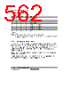
562 / 1158 page  Section 10 16-Bit Timer Pulse Unit (TPU) Rev.1.00 Jun. 07, 2006 Page 510 of 1102 REJ09B0294-0100 Table 10.12 MD3 to MD0 Bit 3 MD3* 1 Bit 2 MD2* 2 Bit 1 MD1 Bit 0 MD0 Description 0 0 0 0 Normal operation 0 0 0 1 Reserved 0 0 1 0 PWM mode 1 0 0 1 1 PWM mode 2 0 1 0 0 Phase counting mode 1 0 1 0 1 Phase counting mode 2 0 1 1 0 Phase counting mode 3 0 1 1 1 Phase counting mode 4 1 X X X [Legend] X: Don't care Notes: 1. MD3 is a reserved bit. The write value should always be 0. 2. Phase counting mode cannot be set for channels 0 and 3. In this case, 0 should always be written to MD2. 10.3.3 Timer I/O Control Register (TIOR) TIOR controls TGR. The TPU has eight TIOR registers, two each for channels 0 and 3, and one each for channels 1, 2, 4, and 5. Care is required since TIOR is affected by the TMDR setting. The initial output specified by TIOR is valid when the counter is stopped (the CST bit in TSTR is cleared to 0). Note also that, in PWM mode 2, the output at the point at which the counter is cleared to 0 is specified. When TGRC or TGRD is designated for buffer operation, this setting is invalid and the register operates as a buffer register. To designate the input capture pin in TIOR, the DDR bit and ICR bit for the corresponding pin should be set to 0 and 1, respectively. For details, see section 9, I/O Ports. |
|
링크 URL |
| ALLDATASHEET 가 귀하에 도움이 되셨나요? [ DONATE ] |
Alldatasheet는? | 광고문의 | 운영자에게 연락하기 | 개인정보취급방침 | 링크 투 데이터시트 | 링크교환 | 제조사별 검색 All Rights Reserved©Alldatasheet.com |
| Russian : Alldatasheetru.com | Korean : Alldatasheet.co.kr | Spanish : Alldatasheet.es | French : Alldatasheet.fr | Italian : Alldatasheetit.com Portuguese : Alldatasheetpt.com | Polish : Alldatasheet.pl | Vietnamese : Alldatasheet.vn Indian : Alldatasheet.in | Mexican : Alldatasheet.com.mx | British : Alldatasheet.co.uk | New Zealand : Alldatasheet.co.nz |
|
Family Site : ic2ic.com |
icmetro.com |
 Korean ▼
 English
 Chinese
 German
 Japanese
 Russian
 Korean
 Spanish
 French
 Italian
 Portuguese
 Polish
 Vietnamese
 Indian
 Mexican
 British
 New Zealand