|
전자부품 데이터시트 검색엔진 |
|
|
전자부품 데이터시트 검색엔진 |
|
H8SX/1663 데이터시트(PDF) 777 Page - Renesas Technology Corp |
|
|
|||||||||||||||||||||||||||||
H8SX/1663 데이터시트(HTML) 777 Page - Renesas Technology Corp |
|
|
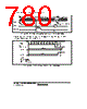
777 / 1158 page  Section 15 Serial Communication Interface (SCI, IrDA, CRC) Rev.1.00 Jun. 07, 2006 Page 725 of 1102 REJ09B0294-0100 15.7.4 Receive Data Sampling Timing and Reception Margin Only the internal clock generated by the on-chip baud rate generator can be used as a transfer clock in smart card interface mode. In this mode, the SCI can operate on a base clock with a frequency of 32, 64, 372, or 256 times the bit rate according to the BCP1 and BCP0 bit settings (the frequency is always 16 times the bit rate in normal asynchronous mode). At reception, the falling edge of the start bit is sampled using the base clock in order to perform internal synchronization. Receive data is sampled on the 16th, 32nd, 186th and 128th rising edges of the base clock so that it can be latched at the middle of each bit as shown in figure 15.28. The reception margin here is determined by the following formula. M = | (0.5 – ) – (L – 0.5) F – (1 + F ) | × 100% 2N 1 N | D – 0.5 | M: Reception margin (%) N: Ratio of bit rate to clock (N = 32, 64, 372, 256) D: Duty cycle of clock (D = 0 to 1.0) L: Frame length (L = 10) F: Absolute value of clock frequency deviation [Legend] Assuming values of F = 0, D = 0.5, and N = 372 in the above formula, the reception margin is determined by the formula below. M = ( 0.5 – ) × 100% = 49.866% 2 × 372 1 Internal basic clock 372 clock cycles 186 clock cycles Receive data (RxD) Synchronization sampling timing D0 D1 Data sampling timing 185 371 0 371 185 0 0 Start bit Figure 15.28 Receive Data Sampling Timing in Smart Card Interface Mode (When Clock Frequency is 372 Times the Bit Rate) |
|
링크 URL |
| ALLDATASHEET 가 귀하에 도움이 되셨나요? [ DONATE ] |
Alldatasheet는? | 광고문의 | 운영자에게 연락하기 | 개인정보취급방침 | 링크 투 데이터시트 | 링크교환 | 제조사별 검색 All Rights Reserved©Alldatasheet.com |
| Russian : Alldatasheetru.com | Korean : Alldatasheet.co.kr | Spanish : Alldatasheet.es | French : Alldatasheet.fr | Italian : Alldatasheetit.com Portuguese : Alldatasheetpt.com | Polish : Alldatasheet.pl | Vietnamese : Alldatasheet.vn Indian : Alldatasheet.in | Mexican : Alldatasheet.com.mx | British : Alldatasheet.co.uk | New Zealand : Alldatasheet.co.nz |
|
Family Site : ic2ic.com |
icmetro.com |
 Korean ▼
 English
 Chinese
 German
 Japanese
 Russian
 Korean
 Spanish
 French
 Italian
 Portuguese
 Polish
 Vietnamese
 Indian
 Mexican
 British
 New Zealand