|
전자부품 데이터시트 검색엔진 |
|
|
전자부품 데이터시트 검색엔진 |
|
ADP1612ARMZ-R7 데이터시트(PDF) 12 Page - Analog Devices |
|
|
|||||||||||||||||||||||||||||
ADP1612ARMZ-R7 데이터시트(HTML) 12 Page - Analog Devices |
|
|
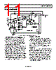
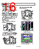
12 / 28 page  ADP1612/ADP1613 Rev. A | Page 12 of 28 THERMAL SHUTDOWN (TSD) The ADP1612/ADP1613 include TSD protection. If the die temperature exceeds 150°C (typical), TSD turns off the NMOS power device, significantly reducing power dissipation in the device and preventing output voltage regulation. The NMOS power device remains off until the die temperature reduces to 130°C (typical). The soft start capacitor is discharged during TSD to ensure low output voltage overshoot and inrush currents when regulation resumes. UNDERVOLTAGE LOCKOUT (UVLO) If the input voltage is below the UVLO threshold, the ADP1612/ ADP1613 automatically turn off the power switch and place the part into a low power consumption mode. This prevents potentially erratic operation at low input voltages and prevents the power device from turning on when the control circuitry cannot operate it. The UVLO levels have ~100 mV of hysteresis to ensure glitch free startup. ENABLE/SHUTDOWN CONTROL The EN input turns the ADP1612/ADP1613 regulator on or off. Drive EN low to turn off the regulator and reduce the input current to 0.01 μA, typical. Drive EN high to turn on the regulator. When the step-up dc-to-dc switching converter is in shutdown mode (EN ≤ 0.3 V), there is a dc path from the input to the output through the inductor and output rectifier. This causes the output voltage to remain slightly below the input voltage by the forward voltage of the rectifier, preventing the output voltage from dropping to ground when the regulator is shutdown. Figure 37 provides a circuit modification to disconnect the output voltage from the input voltage at shutdown. Regardless of the state of the EN pin, when a voltage is applied to VIN of the ADP1612/ADP1613, a large current spike occurs due to the nonisolated path through the inductor and diode between VIN and VOUT. The high current is a result of the output capacitor charging. The peak value is dependent on the inductor, output capacitor, and any load active on the output of the regulator. |
|
|
링크 URL |
| ALLDATASHEET 가 귀하에 도움이 되셨나요? [ DONATE ] |
Alldatasheet는? | 광고문의 | 운영자에게 연락하기 | 개인정보취급방침 | 링크 투 데이터시트 | 링크교환 | 제조사별 검색 All Rights Reserved©Alldatasheet.com |
| Russian : Alldatasheetru.com | Korean : Alldatasheet.co.kr | Spanish : Alldatasheet.es | French : Alldatasheet.fr | Italian : Alldatasheetit.com Portuguese : Alldatasheetpt.com | Polish : Alldatasheet.pl | Vietnamese : Alldatasheet.vn Indian : Alldatasheet.in | Mexican : Alldatasheet.com.mx | British : Alldatasheet.co.uk | New Zealand : Alldatasheet.co.nz |
|
Family Site : ic2ic.com |
icmetro.com |
 Korean ▼
 English
 Chinese
 German
 Japanese
 Russian
 Korean
 Spanish
 French
 Italian
 Portuguese
 Polish
 Vietnamese
 Indian
 Mexican
 British
 New Zealand