|
전자부품 데이터시트 검색엔진 |
|
|
전자부품 데이터시트 검색엔진 |
|
ADRF6655ACPZ-R7 데이터시트(PDF) 39 Page - Analog Devices |
|
|
|||||||||||||||||||||||||||||
ADRF6655ACPZ-R7 데이터시트(HTML) 39 Page - Analog Devices |
|
|
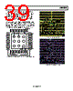
39 / 44 page  ADRF6655 Rev. 0 | Page 39 of 44 The package for the ADRF6655 features an exposed paddle on the underside that should be well soldered to a low thermal and electrical impedance ground plane. This paddle is typically soldered to an exposed opening in the solder mask on the evaluation board. Figure 83 illustrates the dimensions used in the layout of the ADRF6655 footprint on the ADRF6655 evaluation board (1 mil. = 0.0254 mm). Notice the use of nine via holes on the exposed paddle. These ground vias should be connected to all other ground layers on the evaluation board to maximize heat dissipation from the device package. Under these conditions, the thermal impedance of the ADRF6655 was measured to be approximately 29°C/W in still air. .168 .232 .177 .035 .050 .012 .025 .020 Figure 83. Evaluation Board Layout Dimensions for the ADRF6655 Package Figure 84. Evaluation Board Top Layer Figure 85. Evaluation Board Bottom Layer |
|
링크 URL |
| ALLDATASHEET 가 귀하에 도움이 되셨나요? [ DONATE ] |
Alldatasheet는? | 광고문의 | 운영자에게 연락하기 | 개인정보취급방침 | 링크 투 데이터시트 | 링크교환 | 제조사별 검색 All Rights Reserved©Alldatasheet.com |
| Russian : Alldatasheetru.com | Korean : Alldatasheet.co.kr | Spanish : Alldatasheet.es | French : Alldatasheet.fr | Italian : Alldatasheetit.com Portuguese : Alldatasheetpt.com | Polish : Alldatasheet.pl | Vietnamese : Alldatasheet.vn Indian : Alldatasheet.in | Mexican : Alldatasheet.com.mx | British : Alldatasheet.co.uk | New Zealand : Alldatasheet.co.nz |
|
Family Site : ic2ic.com |
icmetro.com |
 Korean ▼
 English
 Chinese
 German
 Japanese
 Russian
 Korean
 Spanish
 French
 Italian
 Portuguese
 Polish
 Vietnamese
 Indian
 Mexican
 British
 New Zealand