|
전자부품 데이터시트 검색엔진 |
|
|
전자부품 데이터시트 검색엔진 |
|
ADRF6655ACPZ-R7 데이터시트(PDF) 7 Page - Analog Devices |
|
|
|||||||||||||||||||||||||||||
ADRF6655ACPZ-R7 데이터시트(HTML) 7 Page - Analog Devices |
|
|
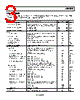
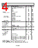
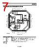
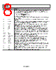
7 / 44 page  ADRF6655 Rev. 0 | Page 7 of 44 PIN CONFIGURATION AND FUNCTION DESPCRIPTIONS VCO LDO 3.3V LDO PD + CHARGE PUMP SERIAL PORT PROGRAMMABLE DIVIDER PRESCALER MODULUS INTEGER FRACTION VCO BAND AND CURRENT CAL/SET PFD 2.5V LDO ÷2 OR ÷3 ÷2 OR ÷4 ×2 NC = NO CONNECT 1 VCC1 2 DECL1 3 CP 4 GND 5 RSET 6 REFIN 7 GND 8 MUXOUT 9 DECL2 10 VCC2 23 GND 24 GND 25 INN 26 INP 27 VCCMIX 28 GND 29 IP3SET 30 GND 22 VCCV2I 21 GND ADRF6655 WIDEBAND UP/DOWN CONVERTER MUX MUX ENABLE VCO CORE 6 6 THIRD-ORDER SDM Figure 3. Pin Configuration Table 4. Pin Function Descriptions Pin No. Mnemonic Description 1 VCC1 Power Supply for Internal 3.3 V LDO. The power supply voltage range is 4.75 V to 5.25 V. Supply pin should be decoupled with 100 pF and 0.1 μF capacitors located close to the pin. 2 DECL1 Decoupling Node for 3.3 V LDO. Pin should be decoupled with 100 pF, 0.1 μF, and 10 μF capacitors located close to the pin. 3 CP Charge Pump Output Pin. Connect this pin to VTUNE through the loop filter. 4, 7, 11, 15, 20, 21, 23, 24, 28, 30, 31, 35, 36 GND Ground. Connect these pins to a low impedance ground plane. |
|
링크 URL |
| ALLDATASHEET 가 귀하에 도움이 되셨나요? [ DONATE ] |
Alldatasheet는? | 광고문의 | 운영자에게 연락하기 | 개인정보취급방침 | 링크 투 데이터시트 | 링크교환 | 제조사별 검색 All Rights Reserved©Alldatasheet.com |
| Russian : Alldatasheetru.com | Korean : Alldatasheet.co.kr | Spanish : Alldatasheet.es | French : Alldatasheet.fr | Italian : Alldatasheetit.com Portuguese : Alldatasheetpt.com | Polish : Alldatasheet.pl | Vietnamese : Alldatasheet.vn Indian : Alldatasheet.in | Mexican : Alldatasheet.com.mx | British : Alldatasheet.co.uk | New Zealand : Alldatasheet.co.nz |
|
Family Site : ic2ic.com |
icmetro.com |
 Korean ▼
 English
 Chinese
 German
 Japanese
 Russian
 Korean
 Spanish
 French
 Italian
 Portuguese
 Polish
 Vietnamese
 Indian
 Mexican
 British
 New Zealand