|
전자부품 데이터시트 검색엔진 |
|
|
전자부품 데이터시트 검색엔진 |
|
M95320-R 데이터시트(PDF) 24 Page - STMicroelectronics |
|
|
|||||||||||||||||||||||||||||
M95320-R 데이터시트(HTML) 24 Page - STMicroelectronics |
|
|
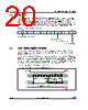
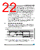
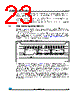
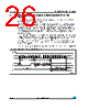
24 / 48 page  Instructions M95320-W M95320-R M95320-DR 24/48 Doc ID 5711 Rev 14 The instruction is not accepted, and is not executed, under the following conditions: ● if the Write Enable Latch (WEL) bit has not been set to 1 (by executing a Write Enable instruction just before), ● if a Write cycle is already in progress, ● if the device has not been deselected, by driving high Chip Select (S), at a byte boundary (after the eighth bit, b0, of the last data byte that has been latched in), ● if the addressed page is in the region protected by the Block Protect (BP1 and BP0) bits. Note: The self-timed write cycle tW is internally executed as a sequence of two consecutive events: [Erase addressed byte(s)], followed by [Program addressed byte(s)]. An erased bit is read as “0” and a programmed bit is read as “1”. Figure 13. Page Write (WRITE) sequence 1. Depending on the memory size, as shown in Table 5, the most significant address bits are Don’t Care. C D AI01796D S 34 33 35 36 37 38 39 40 41 42 44 45 46 47 32 C D S 15 2 1 3456789 10 20 21 22 23 24 25 26 27 14 13 3210 28 29 30 Instruction 16-Bit Address 0 765432 0 1 Data Byte 1 31 43 765432 0 1 Data Byte 2 765432 0 1 Data Byte 3 65432 0 1 Data Byte N |
|
링크 URL |
| ALLDATASHEET 가 귀하에 도움이 되셨나요? [ DONATE ] |
Alldatasheet는? | 광고문의 | 운영자에게 연락하기 | 개인정보취급방침 | 링크 투 데이터시트 | 링크교환 | 제조사별 검색 All Rights Reserved©Alldatasheet.com |
| Russian : Alldatasheetru.com | Korean : Alldatasheet.co.kr | Spanish : Alldatasheet.es | French : Alldatasheet.fr | Italian : Alldatasheetit.com Portuguese : Alldatasheetpt.com | Polish : Alldatasheet.pl | Vietnamese : Alldatasheet.vn Indian : Alldatasheet.in | Mexican : Alldatasheet.com.mx | British : Alldatasheet.co.uk | New Zealand : Alldatasheet.co.nz |
|
Family Site : ic2ic.com |
icmetro.com |
 Korean ▼
 English
 Chinese
 German
 Japanese
 Russian
 Korean
 Spanish
 French
 Italian
 Portuguese
 Polish
 Vietnamese
 Indian
 Mexican
 British
 New Zealand