|
전자부품 데이터시트 검색엔진 |
|
|
전자부품 데이터시트 검색엔진 |
|
STBB2JAD-R 데이터시트(PDF) 7 Page - STMicroelectronics |
|
|
|||||||||||||||||||||||||||||
STBB2JAD-R 데이터시트(HTML) 7 Page - STMicroelectronics |
|
|
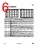
7 / 25 page  DocID022745 Rev 9 7/25 STBB2 Pin configuration BP B4 Bypass mode selection. When EN is high, connecting this pin to a voltage higher than 1.2 V, the device works in bypass mode. A voltage lower than 0.4 V is required to disable bypass mode. In bypass mode VIN is shorted to VOUT through internal switches. Do not leave this pin floating. VSEL D4 Selection of output voltage for fixed versions (0 VOUT = 2.9 V / 1 VOUT = 3.4 V), (0 VOUT = 3.0 V / 1 VOUT = 3.3 V). This feature is not present in the adjustable version where the VSEL pin must be connected to VINA. Do not leave this pin floating. Table 5. Pin description (continued) Pin name Pin n° Description |
|
|
링크 URL |
| ALLDATASHEET 가 귀하에 도움이 되셨나요? [ DONATE ] |
Alldatasheet는? | 광고문의 | 운영자에게 연락하기 | 개인정보취급방침 | 링크 투 데이터시트 | 링크교환 | 제조사별 검색 All Rights Reserved©Alldatasheet.com |
| Russian : Alldatasheetru.com | Korean : Alldatasheet.co.kr | Spanish : Alldatasheet.es | French : Alldatasheet.fr | Italian : Alldatasheetit.com Portuguese : Alldatasheetpt.com | Polish : Alldatasheet.pl | Vietnamese : Alldatasheet.vn Indian : Alldatasheet.in | Mexican : Alldatasheet.com.mx | British : Alldatasheet.co.uk | New Zealand : Alldatasheet.co.nz |
|
Family Site : ic2ic.com |
icmetro.com |
 Korean ▼
 English
 Chinese
 German
 Japanese
 Russian
 Korean
 Spanish
 French
 Italian
 Portuguese
 Polish
 Vietnamese
 Indian
 Mexican
 British
 New Zealand