|
전자부품 데이터시트 검색엔진 |
|
|
전자부품 데이터시트 검색엔진 |
|
UPD6600AGS 데이터시트(PDF) 14 Page - NEC |
|
|
|||||||||||||||||||||||||||||
UPD6600AGS 데이터시트(HTML) 14 Page - NEC |
|
|
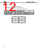
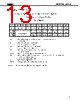
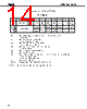
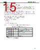
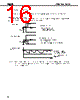
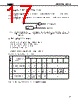
14 / 36 page  µPD6124A, 6600A 14 Table 13-1. Control Register (P1) (2/2) (b) µPD6600A Bit D 9 Name Test mode – Be sure to set 0. 0 1 Set Value Timer D 8 D 7 D 6 D 5 D 4 D 3 D 2 D 1 D 0 HALT D.P. AD MOD K I/O 9 D.P. AD8 RL A A CC 0 ← STOP NOP f /8 AD =0 8 OSC IN RUN OSC STOP f /12 AD =1 8 OSC OUT A 3 S-IN Be sure to set 0. D0 .......................... Specifies data to be input to A0 when the accumulator is shifted to the left. 0: A3, 1:S-IN D1 .......................... Specifies the status of KI/O, as follows: 0: input mode, 1: output mode D2 .......................... Specifies the status of the timer, as follows: 0: Count stop, 1: Count execution D3 .......................... Specifies the carrier frequency output from the REM pin. 0: fOSC/8, 1: fOSC/12 D4 .......................... Specify the MSB of the ROM data pointer. D5 .......................... Be sure to reset them to 0. D6 .......................... Determines what happen to the oscillation circuit when the HALT instruction is executed. 0: Oscillation does not stop 1: Oscillation stops (STOP mode) D7 .......................... Be sure to set this bit to 0. D8, D9 ................. These bits specify test modes. Be sure to set them to 0. Remark D0 = D8 = D9 = 0 on reset, and the other bits are undefined. |
|
링크 URL |
| ALLDATASHEET 가 귀하에 도움이 되셨나요? [ DONATE ] |
Alldatasheet는? | 광고문의 | 운영자에게 연락하기 | 개인정보취급방침 | 링크 투 데이터시트 | 링크교환 | 제조사별 검색 All Rights Reserved©Alldatasheet.com |
| Russian : Alldatasheetru.com | Korean : Alldatasheet.co.kr | Spanish : Alldatasheet.es | French : Alldatasheet.fr | Italian : Alldatasheetit.com Portuguese : Alldatasheetpt.com | Polish : Alldatasheet.pl | Vietnamese : Alldatasheet.vn Indian : Alldatasheet.in | Mexican : Alldatasheet.com.mx | British : Alldatasheet.co.uk | New Zealand : Alldatasheet.co.nz |
|
Family Site : ic2ic.com |
icmetro.com |
 Korean ▼
 English
 Chinese
 German
 Japanese
 Russian
 Korean
 Spanish
 French
 Italian
 Portuguese
 Polish
 Vietnamese
 Indian
 Mexican
 British
 New Zealand