|
전자부품 데이터시트 검색엔진 |
|
|
전자부품 데이터시트 검색엔진 |
|
LTC1709 데이터시트(PDF) 4 Page - Linear Technology |
|
|
|||||||||||||||||||||||||||||
LTC1709 데이터시트(HTML) 4 Page - Linear Technology |
|
|
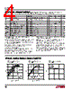
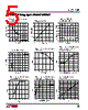
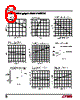
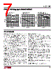
4 / 28 page  4 LTC1709 ELECTRICAL CHARACTERISTICS The q denotes the specifications which apply over the full operating temperature range, otherwise specifications are at TA = 25°C. VIN = 15V, VRUN/SS = 5V unless otherwise noted. Note 6: Rise and fall times are measured using 10% and 90% levels. Delay times are measured using 50% levels. Note 7: The minimum on-time condition corresponds to the on inductor peak-to-peak ripple current ≥40% IMAX (see Minimum On-Time Considerations in the Applications Information section). Note 8: Each built-in pull-up resistor attached to the VID inputs also has a series diode to allow input voltages higher than the VIDVCC supply without damage or clamping (see the Applications Information section). Note 9: When the AMPMD pin is high, the IC pins are connected directly to the internal op amp inputs. When the AMPMD pin is low, internal MOSFET switches connect four 40k resistors around the op amp to create a standard unity-gain differential amp. Note 1: Absolute Maximum Ratings are those values beyond which the life of a device may be impaired. Note 2: The LTC1709EG is guaranteed to meet performance specifications from 0 °C to 70°C. Specifications over the –40°C to 85°C operating temperature range are assured by design, characterization and correlation with statistical process controls. Note 3: TJ is calculated from the ambient temperature TA and power dissipation PD according to the following formulas: LTC1709EG: TJ = TA + (PD • 85°C/W) Note 4: The LTC1709 is tested in a feedback loop that servos VITH to a specified voltage and measures the resultant VEAIN. Note 5: Dynamic supply current is higher due to the gate charge being delivered at the switching frequency. See Applications Information. SYMBOL PARAMETER CONDITIONS MIN TYP MAX UNITS RIN Input Resistance Differential Amp Mode; Measured at VOS+ Input 80 k Ω VOS Input Offset Voltage Op Amp Mode; VCM = 2.5V; VDIFFOUT = 5V; 6 mV IDIFFOUT = 1mA IB Input Bias Current Op Amp Mode 30 200 nA AOL Open Loop DC Gain Op Amp Mode; 0.7V ≤ VDIFFOUT < 10V 5000 V/mV VCM Common Mode Input Voltage Range Op Amp Mode 0 3 V CMRROA Common Mode Rejection Ratio Op Amp Mode; 0V < VCM < 3V 70 90 dB PSRROA Power Supply Rejection Ratio Op Amp Mode; 6V < VIN < 30V 70 90 dB ICL Maximum Output Current Op Amp Mode; VDIFFOUT = 0V 10 35 mA VO(MAX) Maximum Output Voltage Op Amp Mode; IDIFFOUT = 1mA 10 11 V GBW Gain-Bandwidth Product Op Amp Mode; IDIFFOUT = 1mA 2 MHz SR Slew Rate Op Amp Mode; RL = 2k 5 V/ µs TYPICAL PERFOR A CE CHARACTERISTICS Efficiency vs Output Current (Figure 12) Efficiency vs Output Current (Figure 12) Efficiency vs Input Voltage (Figure 12) OUTPUT CURRENT (A) 100 80 60 40 20 0 1709 G01 0.1 1 10 100 VOUT = 2V VEXTVCC = 0V f = 200kHz VIN = 5V VIN = 8V VIN = 12V VIN = 20V OUTPUT CURRENT (A) 1709 G02 100 80 60 40 20 0 0.1 1 10 100 VOUT = 2V VIN = 12V f = 200kHz INTERNAL LDO VS EXTERNALLY APPLIED 5V OVERALL EFFICIENCY (FIGURE 12) VEXTVCC = 5V VEXTVCC = 0V VIN (V) 5 100 90 80 70 1709 G03 10 15 20 VOUT = 3.3V VEXTVCC = 5V IOUT = 20A |
|
|
링크 URL |
| ALLDATASHEET 가 귀하에 도움이 되셨나요? [ DONATE ] |
Alldatasheet는? | 광고문의 | 운영자에게 연락하기 | 개인정보취급방침 | 링크 투 데이터시트 | 링크교환 | 제조사별 검색 All Rights Reserved©Alldatasheet.com |
| Russian : Alldatasheetru.com | Korean : Alldatasheet.co.kr | Spanish : Alldatasheet.es | French : Alldatasheet.fr | Italian : Alldatasheetit.com Portuguese : Alldatasheetpt.com | Polish : Alldatasheet.pl | Vietnamese : Alldatasheet.vn Indian : Alldatasheet.in | Mexican : Alldatasheet.com.mx | British : Alldatasheet.co.uk | New Zealand : Alldatasheet.co.nz |
|
Family Site : ic2ic.com |
icmetro.com |
 Korean ▼
 English
 Chinese
 German
 Japanese
 Russian
 Korean
 Spanish
 French
 Italian
 Portuguese
 Polish
 Vietnamese
 Indian
 Mexican
 British
 New Zealand