|
전자부품 데이터시트 검색엔진 |
|
|
전자부품 데이터시트 검색엔진 |
|
LX1711CDB 데이터시트(PDF) 15 Page - Microsemi Corporation |
|
|
|||||||||||||||||||||||||||||
LX1711CDB 데이터시트(HTML) 15 Page - Microsemi Corporation |
|
|
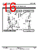
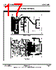
15 / 18 page  LXE1710 EVALUATION BOARD USER GUIDE Microsemi Linfinity Microelectronics Division 11861 Western Avenue, Garden Grove, CA. 92841, 714-898-8121, Fax: 714-893-2570 Page 15 Copyright © 2000 Rev. 1.1, 2000-12-01 PCB LAYOUT RECOMMENDATIONS Like most analog circuits, component placement, signal routing, and power/ground isolation can affect the overall performance of the design. The layout should utilize individual ground traces/planes for the audio amplifier whenever possible. The audio input and controller ground, FET ground, and output filter ground are routed using a “star” connection in the LXE1710 evaluation board. See PCB layer views. The power to the controller IC should be routed using separate traces that do not carry high current pulses from the switching circuit. In general, minimizing the high frequency, high power currents from flowing through the same copper as the audio signal references are recommended. Signal traces that could be sensitive to noise should be node to node connections (no “shared” traces). Stray capacitance at the controller pins RPWM, EAOUT, EAIN, and FAOUT can affect the circuit performance and components associated with these pins should be placed as close to the controller IC as possible. |
|
|
링크 URL |
| ALLDATASHEET 가 귀하에 도움이 되셨나요? [ DONATE ] |
Alldatasheet는? | 광고문의 | 운영자에게 연락하기 | 개인정보취급방침 | 링크 투 데이터시트 | 링크교환 | 제조사별 검색 All Rights Reserved©Alldatasheet.com |
| Russian : Alldatasheetru.com | Korean : Alldatasheet.co.kr | Spanish : Alldatasheet.es | French : Alldatasheet.fr | Italian : Alldatasheetit.com Portuguese : Alldatasheetpt.com | Polish : Alldatasheet.pl | Vietnamese : Alldatasheet.vn Indian : Alldatasheet.in | Mexican : Alldatasheet.com.mx | British : Alldatasheet.co.uk | New Zealand : Alldatasheet.co.nz |
|
Family Site : ic2ic.com |
icmetro.com |
 Korean ▼
 English
 Chinese
 German
 Japanese
 Russian
 Korean
 Spanish
 French
 Italian
 Portuguese
 Polish
 Vietnamese
 Indian
 Mexican
 British
 New Zealand