|
전자부품 데이터시트 검색엔진 |
|
|
전자부품 데이터시트 검색엔진 |
|
ATF331M4 데이터시트(PDF) 3 Page - Agilent(Hewlett-Packard) |
|
|
|||||||||||||||||||||||||||||
ATF331M4 데이터시트(HTML) 3 Page - Agilent(Hewlett-Packard) |
|
|
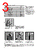
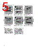
3 / 17 page  2 ATF-331M4 Absolute Maximum Ratings[1] Absolute Symbol Parameter Units Maximum V DS Drain-Source Voltage[2] V 5.5 V GS Gate-Source Voltage[2] V-5 V GD Gate Drain Voltage [2] V-5 I DS Drain Current [2] mA Idiss [3] Pdiss Total Power Dissipation [4] mW 400 Pin max. RF Input Power dBm 20 T CH Channel Temperature[5] °C 160 T STG Storage Temperature °C -65 to 160 θ jc Thermal Resistance [6] °C/W 200 Notes: 1. Operation of this device above any one of these parameters may cause permanent damage. 2. Assumes DC quiescent conditions. 3. V GS = 0 V 4. Source lead temperature is 25 °C. Derate 5 mW/ °C for T L > 40°C. 5. Please refer to failure rates in reliability data sheet to assess the reliability impact of running devices above a channel temperature of 140 °C. 6. Thermal resistance measured using 150 °C Liquid Crystal Measurement method. Product Consistency Distribution Charts [8, 9] VDS (V) Figure 1. Typical Pulsed I-V Curves[7]. (VGS = -0.2 V per step) 02 4 6 8 500 400 300 200 100 0 -0.6 V 0 V +0.6 V NF (dBm) Figure 2. NF @ 2 GHz, 4 V, 60 mA. LSL = 28.5, Nominal = 0.6, USL = 0.8. 0.2 0.4 0.5 0.6 0.7 0.3 0.8 0.9 100 80 60 40 20 0 -3 Std +3 Std Cpk = 1.05 Stdev = 0.07 OIP3 (dBm) Figure 3. OIP3 @ 2 GHz, 4 V, 60 mA. LSL = 28.5, Nominal = 31.0, USL = 36.0 28 32 30 34 36 -3 Std +3 Std 150 120 90 60 30 0 Cpk = 1.00 Stdev = 1.07 GAIN (dB) Figure 4. Gain @ 2 GHz, 4 V, 60 mA. LSL = 13.5, Nominal = 15.0, USL = 16.5 13 15 14 16 17 -3 Std +3 Std 120 100 80 60 40 20 0 Cpk = 4.37 Stdev = 1.11 Notes: 8. Distribution data sample size is 349 samples from 4 different wafers. Future wafers allocated to this product may have nominal values anywhere within the upper and lower spec limits. 9. Measurements made on production test board. This circuit represents a trade-off between an optimal noise match and a realizeable match based on production test requirements. Circuit losses have been de-embedded from actual measurements. Note: 7. Under large signal conditions, V GS may swing positive and the drain current may exceed I dss. These conditions are acceptable as long as the Maximum Pdiss and Pin max ratings are not exceeded. |
|
|
링크 URL |
| ALLDATASHEET 가 귀하에 도움이 되셨나요? [ DONATE ] |
Alldatasheet는? | 광고문의 | 운영자에게 연락하기 | 개인정보취급방침 | 링크 투 데이터시트 | 링크교환 | 제조사별 검색 All Rights Reserved©Alldatasheet.com |
| Russian : Alldatasheetru.com | Korean : Alldatasheet.co.kr | Spanish : Alldatasheet.es | French : Alldatasheet.fr | Italian : Alldatasheetit.com Portuguese : Alldatasheetpt.com | Polish : Alldatasheet.pl | Vietnamese : Alldatasheet.vn Indian : Alldatasheet.in | Mexican : Alldatasheet.com.mx | British : Alldatasheet.co.uk | New Zealand : Alldatasheet.co.nz |
|
Family Site : ic2ic.com |
icmetro.com |
 Korean ▼
 English
 Chinese
 German
 Japanese
 Russian
 Korean
 Spanish
 French
 Italian
 Portuguese
 Polish
 Vietnamese
 Indian
 Mexican
 British
 New Zealand