|
전자부품 데이터시트 검색엔진 |
|
|
전자부품 데이터시트 검색엔진 |
|
ST92185B2 데이터시트(PDF) 9 Page - STMicroelectronics |
|
|
|||||||||||||||||||||||||||||
ST92185B2 데이터시트(HTML) 9 Page - STMicroelectronics |
|
|
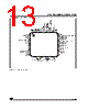
9 / 178 page  9/178 ST92185B - GENERAL DESCRIPTION 1.2 PIN DESCRIPTION RESET Reset (input, active low). The ST9+ is ini- tialised by the Reset signal. With the deactivation of RESET, program execution begins from the Program memory location pointed to by the vector contained in program memory locations 00h and 01h. R/G/B Red/Green/Blue. Video color analog DAC outputs. FB Fast Blanking. Video analog DAC output. VDD Main power supply voltage (5V±10%, digital) VPP: On EPROM/OTP devices, VPP is the pro- gramming voltage pin. VPP should be tied to GND in user mode. MCFM Analog pin for the display pixel frequency multiplier. OSCIN, OSCOUT Oscillator (input and output). These pins connect a parallel-resonant crystal (24MHz maximum), or an external source to the on-chip clock oscillator and buffer. OSCIN is the input of the oscillator inverter and internal clock generator; OSCOUT is the output of the oscillator inverter. VSYNC Vertical Sync. Vertical video synchronisa- tion input to OSD. Positive or negative polarity. HSYNC/CSYNC Horizontal/Composite sync. Hori- zontal or composite video synchronisation input to OSD. Positive or negative polarity. PXFM Analog pin for the Display Pixel Frequency Multiplier AVDD3 Analog VDD of PLL. This pin must be tied to VDD externally. GND Digital circuit ground. AGND Analog circuit ground (must be tied exter- nally to digital GND). AVDD1, AVDD2 Analog power supplies (must be tied externally to VDD). CVBSO, JTDO, JTCK, JTMS Test pins: leave floating. TEST0 Test pin: must be tied to AVDD2. JTRST0 Test pin: must be tied to GND. Figure 2. 56-Pin Package Pin-Out INT7/P2.0 RESET P0.7 P0.6 P0.5 P0.4 P0.3 AIN4/P0.2 P0.1 P0.0 CSO/RESET0/P3.7 P3.6 P3.5 P3.4 B G R FB SDI/SDO/P5.1 SCK/INT2/P5.0 VDD JTDO N.C VPP AVDD3 TEST0 MCFM JTCK P2.1/INT5/AIN1 P2.2/INT0/AIN2 P2.3/INT6/VS01 P2.4/NMI P2.5/AIN3/INT4/VS02 OSCIN OSCOUT P4.7/PWM7/EXTRG/STOUT P4.6/PWM6 P4.5/PWM5 P4.4/PWM4 P4.3/PWM3/TSLU/HT P4.2/PWM2 P4.1/PWM1 P4.0/PWM0 VSYNC HSYNC/CSYNC AVDD1 PXFM JTRSTO GND AGND N.C N.C JTMS AVDD2 CVBSO N.C 1 2 3 4 5 6 7 8 9 10 11 12 13 14 15 16 17 18 19 20 21 22 23 24 25 26 27 28 56 55 54 53 52 51 50 49 48 47 46 45 44 43 42 41 40 39 38 37 36 35 34 33 32 31 30 29 |
|
링크 URL |
| ALLDATASHEET 가 귀하에 도움이 되셨나요? [ DONATE ] |
Alldatasheet는? | 광고문의 | 운영자에게 연락하기 | 개인정보취급방침 | 링크 투 데이터시트 | 링크교환 | 제조사별 검색 All Rights Reserved©Alldatasheet.com |
| Russian : Alldatasheetru.com | Korean : Alldatasheet.co.kr | Spanish : Alldatasheet.es | French : Alldatasheet.fr | Italian : Alldatasheetit.com Portuguese : Alldatasheetpt.com | Polish : Alldatasheet.pl | Vietnamese : Alldatasheet.vn Indian : Alldatasheet.in | Mexican : Alldatasheet.com.mx | British : Alldatasheet.co.uk | New Zealand : Alldatasheet.co.nz |
|
Family Site : ic2ic.com |
icmetro.com |
 Korean ▼
 English
 Chinese
 German
 Japanese
 Russian
 Korean
 Spanish
 French
 Italian
 Portuguese
 Polish
 Vietnamese
 Indian
 Mexican
 British
 New Zealand