|
전자부품 데이터시트 검색엔진 |
|
|
전자부품 데이터시트 검색엔진 |
|
MIPSZ2012D2R2 데이터시트(PDF) 30 Page - STMicroelectronics |
|
|
|||||||||||||||||||||||||||||
MIPSZ2012D2R2 데이터시트(HTML) 30 Page - STMicroelectronics |
|
|
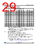
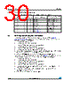
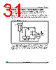
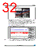
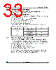
30 / 48 page  Application information TS4621B 30/48 Doc ID 022194 Rev 2 4.1.5 Summary of output impedance 4.2 Wake-up and standby time definition The wake-up time of the TS4621B is guaranteed at 12 ms typical (refer to Chapter 3: Electrical characteristics). However, since the TS4621B is activated with an I2C bus, the wake-up start procedure is as follows. 1. The master sends a start bit. 2. The master sends the device address. 3. The slave (TS4621B) answers by an acknowledge bit. 4. The master sends the register address. 5. The slave (TS4621B) answers by an acknowledge bit. 6. The master sends the output mode configuration (CR1). 7. If the TS4621B was previously in standby mode, the wake-up starts on the falling edge of the eighth clock signal (SCL) corresponding to the CR1 byte. 8. After 12 ms (de-pop sequence time), the TS4621B outputs are operational. The standby time is guaranteed as 100 µs typical (refer to Chapter 3). However, since the TS4621B is de-activated with an I2C bus, the standby time operates as follows. 1. The master sends a start bit. 2. The master sends the device address. 3. The slave (TS4621B) answers by an acknowledge bit. 4. The master sends the register address. 5. The slave (TS4621B) answers by an acknowledge bit. 6. The master sends the output mode configuration (CR1), which corresponds, in this case, to standby mode. 7. The standby time starts on the falling edge of the eighth clock signal (SCL) corresponding to the CR1 byte. 8. After 100 µs, the TS4621B is in standby mode. Table 13. Summary table for output impedance vs. output mode SWS HiZ HP_EN Output impedance Maximum voltage allowed on output pin 1 0 0 20 to 40 Ω Less than ± 100 mV 1 0 1 20 to 40 Ω Less than ± 100 mV 1 1 0 about 10 k Ω -0.3 V to AVdd 1 1 1 about 10 k Ω -0.3 V to AVdd 0 0 0 20 to 40 Ω Less than ± 100 mV 0 0 1 Less than 1 Ω Not applicable 0 1 0 See Figure 18 -1.8 to +1.8 V 0 1 1 See Figure 18 -1.8 to +1.8 V |
|
링크 URL |
| ALLDATASHEET 가 귀하에 도움이 되셨나요? [ DONATE ] |
Alldatasheet는? | 광고문의 | 운영자에게 연락하기 | 개인정보취급방침 | 링크 투 데이터시트 | 링크교환 | 제조사별 검색 All Rights Reserved©Alldatasheet.com |
| Russian : Alldatasheetru.com | Korean : Alldatasheet.co.kr | Spanish : Alldatasheet.es | French : Alldatasheet.fr | Italian : Alldatasheetit.com Portuguese : Alldatasheetpt.com | Polish : Alldatasheet.pl | Vietnamese : Alldatasheet.vn Indian : Alldatasheet.in | Mexican : Alldatasheet.com.mx | British : Alldatasheet.co.uk | New Zealand : Alldatasheet.co.nz |
|
Family Site : ic2ic.com |
icmetro.com |
 Korean ▼
 English
 Chinese
 German
 Japanese
 Russian
 Korean
 Spanish
 French
 Italian
 Portuguese
 Polish
 Vietnamese
 Indian
 Mexican
 British
 New Zealand