|
전자부품 데이터시트 검색엔진 |
|
|
전자부품 데이터시트 검색엔진 |
|
ADP1610ARMZ-R7 데이터시트(PDF) 4 Page - Analog Devices |
|
|
|||||||||||||||||||||||||||||
ADP1610ARMZ-R7 데이터시트(HTML) 4 Page - Analog Devices |
|
|
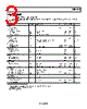
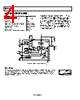
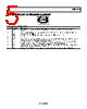
4 / 16 page  ADP1610 Rev. 0 | Page 4 of 16 ABSOLUTE MAXIMUM RATINGS Table 2. Parameter Rating IN, COMP, SD, SS, RT, FB to GND −0.3 V to +6 V SW to GND 14 V RMS SW Pin Current 1.2 A Operating Ambient Temperature Range −40°C to +85°C Operating Junction Temperature Range −40°C to +125°C Storage Temperature Range −65°C to +150°C θJA, Two Layers 206°C/W θJA, Four Layers 142°C/W Lead Temperature Range (Soldering, 60 s) 300°C Stresses above those listed under Absolute Maximum Ratings may cause permanent damage to the device. This is a stress rating only and functional operation of the device at these or any other conditions above those indicated in the operational section of this specification is not implied. Exposure to absolute maximum rating conditions for extended periods may affect device reliability. Absolute maximum ratings apply individually only, not in combination. Unless otherwise specified, all other voltages are referenced to GND. REF RAMP GEN Q S R F/F DRIVER CURRENT SENSE AMPLIFIER COMP SW FB IN COMPARATOR ERROR AMP GND BIAS gm SD SS VOUT ADP1610 IN VOUT OSC SOFT START RT R1 R2 CSS CC CIN COUT D1 L1 RC VIN 1.2MHz 700kHz 1 6 5 4 3 7 2 8 Figure 2. Block Diagram and Typical Application Circuit ESD CAUTION ESD (electrostatic discharge) sensitive device. Electrostatic charges as high as 4000 V readily accumulate on the human body and test equipment and can discharge without detection. Although this product features proprietary ESD protection circuitry, permanent damage may occur on devices subjected to high energy electrostatic discharges. Therefore, proper ESD precautions are recommended to avoid performance degradation or loss of functionality. |
|
|
링크 URL |
| ALLDATASHEET 가 귀하에 도움이 되셨나요? [ DONATE ] |
Alldatasheet는? | 광고문의 | 운영자에게 연락하기 | 개인정보취급방침 | 링크 투 데이터시트 | 링크교환 | 제조사별 검색 All Rights Reserved©Alldatasheet.com |
| Russian : Alldatasheetru.com | Korean : Alldatasheet.co.kr | Spanish : Alldatasheet.es | French : Alldatasheet.fr | Italian : Alldatasheetit.com Portuguese : Alldatasheetpt.com | Polish : Alldatasheet.pl | Vietnamese : Alldatasheet.vn Indian : Alldatasheet.in | Mexican : Alldatasheet.com.mx | British : Alldatasheet.co.uk | New Zealand : Alldatasheet.co.nz |
|
Family Site : ic2ic.com |
icmetro.com |
 Korean ▼
 English
 Chinese
 German
 Japanese
 Russian
 Korean
 Spanish
 French
 Italian
 Portuguese
 Polish
 Vietnamese
 Indian
 Mexican
 British
 New Zealand