|
전자부품 데이터시트 검색엔진 |
|
|
전자부품 데이터시트 검색엔진 |
|
ADP1610ARMZ-R7 데이터시트(PDF) 15 Page - Analog Devices |
|
|
|||||||||||||||||||||||||||||
ADP1610ARMZ-R7 데이터시트(HTML) 15 Page - Analog Devices |
|
|
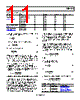
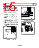
15 / 16 page  ADP1610 Rev. 0 | Page 15 of 16 LAYOUT PROCEDURE To get high efficiency, good regulation, and stability, a well- designed printed circuit board layout is required. Where possible, use the sample application board layout as a model. Follow these guidelines when designing printed circuit boards (see Figure 1): • Keep the low ESR input capacitor, CIN, close to IN and GND. • Keep the high current path from CIN through the inductor L1 to SW and PGND as short as possible. • Keep the high current path from CIN through L1, the rectifier D1, and the output capacitor COUT as short as possible. • Keep high current traces as short and as wide as possible. • Place the feedback resistors as close to the FB pin as possible to prevent noise pickup. • Place the compensation components as close as possible to COMP. • Avoid routing high impedance traces near any node connected to SW or near the inductor to prevent radiated noise injection. Figure 31. Sample Application Board (Bottom Layer) Figure 32. Sample Application Board (Top Layer) Figure 33. Sample Application Board (Silkscreen Layer) |
|
|
링크 URL |
| ALLDATASHEET 가 귀하에 도움이 되셨나요? [ DONATE ] |
Alldatasheet는? | 광고문의 | 운영자에게 연락하기 | 개인정보취급방침 | 링크 투 데이터시트 | 링크교환 | 제조사별 검색 All Rights Reserved©Alldatasheet.com |
| Russian : Alldatasheetru.com | Korean : Alldatasheet.co.kr | Spanish : Alldatasheet.es | French : Alldatasheet.fr | Italian : Alldatasheetit.com Portuguese : Alldatasheetpt.com | Polish : Alldatasheet.pl | Vietnamese : Alldatasheet.vn Indian : Alldatasheet.in | Mexican : Alldatasheet.com.mx | British : Alldatasheet.co.uk | New Zealand : Alldatasheet.co.nz |
|
Family Site : ic2ic.com |
icmetro.com |
 Korean ▼
 English
 Chinese
 German
 Japanese
 Russian
 Korean
 Spanish
 French
 Italian
 Portuguese
 Polish
 Vietnamese
 Indian
 Mexican
 British
 New Zealand