|
전자부품 데이터시트 검색엔진 |
|
|
전자부품 데이터시트 검색엔진 |
|
ISL9301IRZ 데이터시트(PDF) 10 Page - Renesas Technology Corp |
|
|
|||||||||||||||||||||||||||||
ISL9301IRZ 데이터시트(HTML) 10 Page - Renesas Technology Corp |
|
|
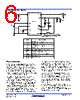
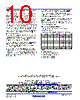
10 / 12 page  FN6435 Rev 3.00 Page 10 of 12 September 21, 2011 ISL9301 Intersil products are manufactured, assembled and tested utilizing ISO9001 quality systems as noted in the quality certifications found at www.intersil.com/en/support/qualandreliability.html Intersil products are sold by description only. Intersil may modify the circuit design and/or specifications of products at any time without notice, provided that such modification does not, in Intersil's sole judgment, affect the form, fit or function of the product. Accordingly, the reader is cautioned to verify that datasheets are current before placing orders. Information furnished by Intersil is believed to be accurate and reliable. However, no responsibility is assumed by Intersil or its subsidiaries for its use; nor for any infringements of patents or other rights of third parties which may result from its use. No license is granted by implication or otherwise under any patent or patent rights of Intersil or its subsidiaries. For information regarding Intersil Corporation and its products, see www.intersil.com For additional products, see www.intersil.com/en/products.html © Copyright Intersil Americas LLC 2008-2011. All Rights Reserved. All trademarks and registered trademarks are the property of their respective owners. VOUT is regulated at 4.5V, the charger is ON, delivering a trickle charge current. The IC moves to a fast charge constant current mode when VBAT reaches the VMIN threshold. There are 3 possible states in this mode depending on the output current. When the sum of the output current and the fast charge current is smaller than the input current limit, the IC enters the Fast Charge state with the charge current set by RIREF. When the output current and the fast charge current are greater than the input current limit, the IC will enter the PPM mode, where the charging current is reduced to a point such that the sum of output current and the charging current equals to the input current limit. If the output current by itself is greater than the input current limit, the IC enters the Battery Discharge state, where the battery is discharged to the system to supply a part of the output demand. When the battery voltage reaches 4.2V, the IC enters the CV Charge state, where PPR is LO, CHG is LO and VOUT is regulated at 4.5V. The battery is being charged at a constant voltage while the charging current decreases. When the charging current is reduced to the IMIN threshold, the IC enters a Charge Complete state, where PPR is LO, CHG is HI, VOUT is regulated at 4.5V and the charger continues to charge the battery. When the timeout interval has elapsed after the Charge Complete state, the IC will enter the Disabled state, where the PPR is LO, CHG is HI, VOUT is regulated at 4.5V and the charger is OFF. After the Charge Complete state, if VBAT is below the re-charge threshold, the IC will re-initialize and start a new cycle. If the timeout limit is reached before the Charge Complete state, the IC enters the Charger Fault state, where PPR is LO, CHG is blinking, VOUT is regulated at 4.5V and the charger is OFF. This state is latched until the input power is removed and re-applied to start a new cycle. Any time during the operation, if the die temperature reaches the OTP threshold, the IC will enter the OTP state, where PPR is LO, CHG is HI, and the charger is OFF. VOUT is disconnected from VIN and connected to VBAT internally to maintain system power need. Summary of Output States The output states under various fault conditions are summarized in Table 1. TABLE 1. OUTPUT STATES UNDER FAULT CONDITIONS OTP OVP BATON M1 M2 Y Y H OFF ON Y N H OFF ON N Y H OFF ON Y Y L OFF OFF Y N L OFF OFF N Y L OFF OFF N N X Regulating Charging NOTES: 1. BATON: BATON Pin 2. OVP: Input Overvoltage Protection 3. OTP: Over-Temperature Protection 4. M1: Output Path MOSFET 5. M2: Battery Path MOSFET |
|
|
링크 URL |
| ALLDATASHEET 가 귀하에 도움이 되셨나요? [ DONATE ] |
Alldatasheet는? | 광고문의 | 운영자에게 연락하기 | 개인정보취급방침 | 링크 투 데이터시트 | 링크교환 | 제조사별 검색 All Rights Reserved©Alldatasheet.com |
| Russian : Alldatasheetru.com | Korean : Alldatasheet.co.kr | Spanish : Alldatasheet.es | French : Alldatasheet.fr | Italian : Alldatasheetit.com Portuguese : Alldatasheetpt.com | Polish : Alldatasheet.pl | Vietnamese : Alldatasheet.vn Indian : Alldatasheet.in | Mexican : Alldatasheet.com.mx | British : Alldatasheet.co.uk | New Zealand : Alldatasheet.co.nz |
|
Family Site : ic2ic.com |
icmetro.com |
 Korean ▼
 English
 Chinese
 German
 Japanese
 Russian
 Korean
 Spanish
 French
 Italian
 Portuguese
 Polish
 Vietnamese
 Indian
 Mexican
 British
 New Zealand