|
전자부품 데이터시트 검색엔진 |
|
|
전자부품 데이터시트 검색엔진 |
|
NCV7728DPAR2G 데이터시트(PDF) 26 Page - ON Semiconductor |
|
|
|||||||||||||||||||||||||||||
NCV7728DPAR2G 데이터시트(HTML) 26 Page - ON Semiconductor |
|
|
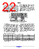
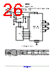
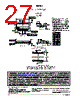
26 / 27 page  NCV7728 www.onsemi.com 26 APPLICATION DIAGRAM The application drawing below demonstrates the drive capability of the NCV7728. The VS1 and VS2 pins must be tied together to avoid any potential difference in the supply voltage. NCV7728 Hex Half Bridge GND GND GND EN VCC SI SO SCLK CSB VS1 VS2 OUT1 OUT2 M1 OUT3 OUT4 M2 OUT5 OUT6 M3 uC EN MOSI MISO SCLK CSB NCV8518B DELAY WDI VOUT EN GND VCC VIN 20k 120k RESET IO RESET MRA4003T3 0.1uF 13.2V 1.0uF GND M5 M4 Figure 29. Application Drawing ORDERING INFORMATION Device Markiing Package Shipping† NCV7728DPR2G NCV7728 SSOP24 (Pb−Free) 2500 / Tape & Reel NCV7728DPAR2G NCV7728A †For information on tape and reel specifications, including part orientation and tape sizes, please refer to our Tape and Reel Packaging Specifications Brochure, BRD8011/D. |
|
|
링크 URL |
| ALLDATASHEET 가 귀하에 도움이 되셨나요? [ DONATE ] |
Alldatasheet는? | 광고문의 | 운영자에게 연락하기 | 개인정보취급방침 | 링크 투 데이터시트 | 링크교환 | 제조사별 검색 All Rights Reserved©Alldatasheet.com |
| Russian : Alldatasheetru.com | Korean : Alldatasheet.co.kr | Spanish : Alldatasheet.es | French : Alldatasheet.fr | Italian : Alldatasheetit.com Portuguese : Alldatasheetpt.com | Polish : Alldatasheet.pl | Vietnamese : Alldatasheet.vn Indian : Alldatasheet.in | Mexican : Alldatasheet.com.mx | British : Alldatasheet.co.uk | New Zealand : Alldatasheet.co.nz |
|
Family Site : ic2ic.com |
icmetro.com |
 Korean ▼
 English
 Chinese
 German
 Japanese
 Russian
 Korean
 Spanish
 French
 Italian
 Portuguese
 Polish
 Vietnamese
 Indian
 Mexican
 British
 New Zealand