|
전자부품 데이터시트 검색엔진 |
|
|
전자부품 데이터시트 검색엔진 |
|
AT89C51ED2-RDTIM 데이터시트(PDF) 18 Page - ATMEL Corporation |
|
|
|||||||||||||||||||||||||||||
AT89C51ED2-RDTIM 데이터시트(HTML) 18 Page - ATMEL Corporation |
|
|
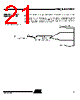
18 / 137 page  18 AT89C51RD2/ED2 4235E–8051–04/04 Figure 6. Mode Switching Waveforms The X2 bit in the CKCON0 register (see Table 16) allows a switch from 12 clock periods per instruction to 6 clock periods and vice versa. At reset, the speed is set according to X2 bit of Hardware Security Byte (HSB). By default, Standard mode is active. Setting the X2 bit activates the X2 feature (X2 mode). The T0X2, T1X2, T2X2, UartX2, PcaX2, and WdX2 bits in the CKCON0 register (Table 16) and SPIX2 bit in the CKCON1 register (see Table 17) allows a switch from standard peripheral speed (12 clock periods per peripheral clock cycle) to fast peripheral speed (6 clock periods per peripheral clock cycle). These bits are active only in X2 mode. XTAL1:2 XTAL1 CPU Clock X2 Bit X2 Mode STD Mode STD Mode FOSC |
|
링크 URL |
| ALLDATASHEET 가 귀하에 도움이 되셨나요? [ DONATE ] |
Alldatasheet는? | 광고문의 | 운영자에게 연락하기 | 개인정보취급방침 | 링크 투 데이터시트 | 링크교환 | 제조사별 검색 All Rights Reserved©Alldatasheet.com |
| Russian : Alldatasheetru.com | Korean : Alldatasheet.co.kr | Spanish : Alldatasheet.es | French : Alldatasheet.fr | Italian : Alldatasheetit.com Portuguese : Alldatasheetpt.com | Polish : Alldatasheet.pl | Vietnamese : Alldatasheet.vn Indian : Alldatasheet.in | Mexican : Alldatasheet.com.mx | British : Alldatasheet.co.uk | New Zealand : Alldatasheet.co.nz |
|
Family Site : ic2ic.com |
icmetro.com |
 Korean ▼
 English
 Chinese
 German
 Japanese
 Russian
 Korean
 Spanish
 French
 Italian
 Portuguese
 Polish
 Vietnamese
 Indian
 Mexican
 British
 New Zealand