|
전자부품 데이터시트 검색엔진 |
|
|
전자부품 데이터시트 검색엔진 |
|
AD9739-R2-EBZ 데이터시트(PDF) 11 Page - Analog Devices |
|
|
|||||||||||||||||||||||||||||
AD9739-R2-EBZ 데이터시트(HTML) 11 Page - Analog Devices |
|
|
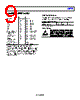
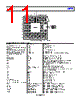
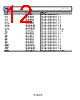
11 / 50 page  Data Sheet AD9739 Rev. E | Page 11 of 50 A B C D E F G H J K L M N P 14 13 12 11 10 6 3 2 1 9 5 4 IRQ CS SCLK RESET SDIO SDO 7 8 I120 VREF AD9739 Figure 6. Analog I/O and SPI Control Pins (Top View) Table 7. AD9739 Pin Function Descriptions Pin No. Mnemonic Description C1, C2, D1, D2, E1, E2, E3, E4 VDDC 1.8 V Clock Supply Input. A1, A2, A3, A4, A5, B1, B2, B3, B4, B5, C4, C5, D4, D5 VSSC Clock Supply Return. A10, A11, B10, B11, C10, C11, D10, D11 VDDA 3.3 V Analog Supply Input. A12, A13, B12, B13, C12, C13, D12, D13, VSSA Analog Supply Return. A6, A9, B6, B9, C6, C9, D6, D9, F1, F2, F3, F4, E11, E12, E13, E14, F11, F12 VSSA Shield Analog Supply Return Shield. Tie to VSSA at the DAC. A14 NC No Connect. Do not connect to this pin. A7, B7, C7, D7 IOUTN DAC Negative Current Output Source. A8, B8, C8, D8 IOUTP DAC Positive Current Output Source. B14 I120 Nominal 1.2 V Reference. Tie to analog ground via a 10 kΩ resistor to generate a 120 µA reference current. C14 VREF Voltage Reference Input/Output. Decouple to VSSA with a 1 nF capacitor. D14 NC Factory Test Pin. Do not connect to this pin. C3, D3 DACCLK_N/DACCLK_P Negative/Positive DAC Clock Input (DACCLK). F13 IRQ Interrupt Request Open Drain Output. Active high. Pull up to VDD33 with a 10 kΩ resistor. F14 RESET Reset Input. Active high. Tie to VSS if unused. G13 CS Serial Port Enable Input. G14 SDIO Serial Port Data Input/Output. H13 SCLK Serial Port Clock Input. H14 SDO Serial Port Data Output. J3, J4, J11, J12 VDD33 3.3 V Digital Supply Input. G1, G2, G3, G4, G11, G12 VDD 1.8 V Digital Supply. Input. H1, H2, H3, H4, H11, H12, K3, K4, K11, K12 VSS Digital Supply Return. J1, J2 SYNC_OUT_P/SYNC_OUT_N Positive/Negative SYNC Output (SYNC_OUT) K1, K2 SYNC_IN_P/SYNC_IN_N Positive/Negative SYNC Input (SYNC_IN) J13, J14 DCO_P/DCO_N Positive/Negative Data Clock Output (DCO). K13, K14 DCI_P/DCI_N Positive/Negative Data Clock Input (DCI). L1, M1 DB1[0]P/DB1[0]N Port 1 Positive/Negative Data Input Bit 0, LSB. L2, M2 DB1[1]P/DB1[1]N Port 1 Positive/Negative Data Input Bit 1. L3, M3 DB1[2]P/DB1[2]N Port 1 Positive/Negative Data Input Bit 2. |
|
링크 URL |
| ALLDATASHEET 가 귀하에 도움이 되셨나요? [ DONATE ] |
Alldatasheet는? | 광고문의 | 운영자에게 연락하기 | 개인정보취급방침 | 링크 투 데이터시트 | 링크교환 | 제조사별 검색 All Rights Reserved©Alldatasheet.com |
| Russian : Alldatasheetru.com | Korean : Alldatasheet.co.kr | Spanish : Alldatasheet.es | French : Alldatasheet.fr | Italian : Alldatasheetit.com Portuguese : Alldatasheetpt.com | Polish : Alldatasheet.pl | Vietnamese : Alldatasheet.vn Indian : Alldatasheet.in | Mexican : Alldatasheet.com.mx | British : Alldatasheet.co.uk | New Zealand : Alldatasheet.co.nz |
|
Family Site : ic2ic.com |
icmetro.com |
 Korean ▼
 English
 Chinese
 German
 Japanese
 Russian
 Korean
 Spanish
 French
 Italian
 Portuguese
 Polish
 Vietnamese
 Indian
 Mexican
 British
 New Zealand