|
전자부품 데이터시트 검색엔진 |
|
|
전자부품 데이터시트 검색엔진 |
|
AD9739-R2-EBZ 데이터시트(PDF) 24 Page - Analog Devices |
|
|
|||||||||||||||||||||||||||||
AD9739-R2-EBZ 데이터시트(HTML) 24 Page - Analog Devices |
|
|
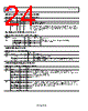
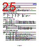
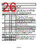
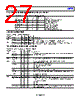
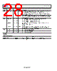
24 / 50 page  AD9739 Data Sheet Rev. E | Page 24 of 50 SPI PORT CONFIGURATION AND SOFTWARE RESET Table 10. SPI Port Configuration and Software Reset Register Address (Hex) Name Bit R/W Default Setting Comments 0x00 SDIO_DIR 7 R/W 0 0 = 4-wire SPI, 1 = 3-wire SPI. LSB/MSB 6 R/W 0 0 = MSB first, 1 = LSB first. Reset 5 R/W 0 Software reset is recommended before modification of other SPI registers from the default setting. Setting the bit to 1 causes all registers (except 0x00) to be set to the default setting. Setting the bit to 0 corresponds to the inactive state, allowing the user to modify registers from the default setting. POWER-DOWN LVDS INTERFACE AND TXDAC® Table 11. Power-Down LVDS Interface and TxDAC Register Address (Hex) Name Bit R/W Default Setting Comments 0x01 LVDS_DRVR_PD 5 R/W 0 Power-down of the LVDS drivers/receivers and TxDAC. 0 = enable, 1 = disable. LVDS_RCVR_PD 4 R/W 0 CLK_RCVR_PD 1 R/W 0 DAC_BIAS_PD 0 R/W 0 CONTROLLER CLOCK DISABLE Table 12. Controller Clock Disable Register Address (Hex) Name Bit R/W Default Setting Comments 0x02 CLKGEN_PD 3 R/W 0 Internal CLK distribution enable: 0 = enable, 1 = disable. REC_CNT_CLK 1 R/W 1 LVDS receiver (REC_CNT_CLK) and mu controller clock disable (MU_CNT_CLK). 0 = disable, 1 = enable. MU_CNT_CLK 0 R/W 1 INTERRUPT REQUEST (IRQ) ENABLE/STATUS Table 13. Interrupt Request (IRQ) Enable/Status Register Address (Hex) Name Bit R/W Default Setting Comments 0x03 SYNC_LST_EN 5 W 0 This register enables the sync, mu, and LVDS Rx controllers to update their corresponding IRQ status bits in Register 0x04, which defines whether the controller is locked (LCK) or unlocked (LST). 0 = disable (resets the status bit). 1 = enable. SYNC_LCK_EN 4 W 0 MU_LST_EN 3 W 0 MU_LCK_EN 2 W 0 RCV_LST_EN 1 W 0 RCV_LCK_EN 0 W 0 0x04 SYNC_LST_IRQ 5 R 0 This register indicates the status of the controllers. For LCK_IQR bits: 0 = lost locked, 1 = locked. For LST_IQR bits: 0 = not lost locked, 1 = unlocked. Note that, if the controller IRQ is serviced, the relevant bits in Register 0x03 should be reset by writing 0, followed by another write of 1 to enable. SYNC_LCK_IRQ 4 R 0 MU_LST_IRQ 3 R 0 MU_LCK_IRQ 2 R 0 RCV_LST_IRQ 1 R 0 RCV_LCK_IRQ 0 R 0 |
|
링크 URL |
| ALLDATASHEET 가 귀하에 도움이 되셨나요? [ DONATE ] |
Alldatasheet는? | 광고문의 | 운영자에게 연락하기 | 개인정보취급방침 | 링크 투 데이터시트 | 링크교환 | 제조사별 검색 All Rights Reserved©Alldatasheet.com |
| Russian : Alldatasheetru.com | Korean : Alldatasheet.co.kr | Spanish : Alldatasheet.es | French : Alldatasheet.fr | Italian : Alldatasheetit.com Portuguese : Alldatasheetpt.com | Polish : Alldatasheet.pl | Vietnamese : Alldatasheet.vn Indian : Alldatasheet.in | Mexican : Alldatasheet.com.mx | British : Alldatasheet.co.uk | New Zealand : Alldatasheet.co.nz |
|
Family Site : ic2ic.com |
icmetro.com |
 Korean ▼
 English
 Chinese
 German
 Japanese
 Russian
 Korean
 Spanish
 French
 Italian
 Portuguese
 Polish
 Vietnamese
 Indian
 Mexican
 British
 New Zealand