|
전자부품 데이터시트 검색엔진 |
|
|
전자부품 데이터시트 검색엔진 |
|
HM24C32 데이터시트(PDF) 7 Page - Shenzhen Huazhimei Semiconductor Co., Ltd |
|
|
|||||||||||||||||||||||||||||
HM24C32 데이터시트(HTML) 7 Page - Shenzhen Huazhimei Semiconductor Co., Ltd |
|
|
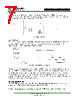
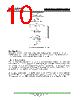
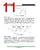
7 / 16 page  HM24C32/HM24C64 7 Bit Transfer One data bit is transferred during each clock pulse. The data on the SDA line must remain stable during the HIGH period of the clock pulse as changes in the data line at this time will be interpreted as a control signal, as shown in Figure 6. Figure 6. Bit Transfer Acknowledge Each receiving device, when addressed, is obliged to generate an acknowledgement after the reception of each byte. The master device must generate an extra clock pulse which is associated with this acknowledge bit (see Figure 7). Figure 7. Acknowledge on the I2C bus The device that acknowledges must pull down the SDA line during the acknowledge clock pulse, so that the SDA line is stable LOW during the HIGH period of the acknowledge related clock pulse (set-up and hold times must be taken into consideration). A master receiver must signal an end of data to the transmitter by not generating an acknowledgement on the last byte that has been clocked out of the slave. In this event the transmitter must leave the data line HIGH to enable the master to generate a stop condition. DEVICE ADDRESSING The EEPROM devices all require an 8-bit device address word following a start condition to enable the chip for a read or write operation (see to Figure 8). The device address word consists of a mandatory "1", "0" sequence for the first four most Shenzhen H&M Semiconductor Co.Ltd http://www.hmsemi.com |
|
|
링크 URL |
| ALLDATASHEET 가 귀하에 도움이 되셨나요? [ DONATE ] |
Alldatasheet는? | 광고문의 | 운영자에게 연락하기 | 개인정보취급방침 | 링크 투 데이터시트 | 링크교환 | 제조사별 검색 All Rights Reserved©Alldatasheet.com |
| Russian : Alldatasheetru.com | Korean : Alldatasheet.co.kr | Spanish : Alldatasheet.es | French : Alldatasheet.fr | Italian : Alldatasheetit.com Portuguese : Alldatasheetpt.com | Polish : Alldatasheet.pl | Vietnamese : Alldatasheet.vn Indian : Alldatasheet.in | Mexican : Alldatasheet.com.mx | British : Alldatasheet.co.uk | New Zealand : Alldatasheet.co.nz |
|
Family Site : ic2ic.com |
icmetro.com |
 Korean ▼
 English
 Chinese
 German
 Japanese
 Russian
 Korean
 Spanish
 French
 Italian
 Portuguese
 Polish
 Vietnamese
 Indian
 Mexican
 British
 New Zealand