|
전자부품 데이터시트 검색엔진 |
|
|
전자부품 데이터시트 검색엔진 |
|
AD6432 데이터시트(PDF) 14 Page - Analog Devices |
|
|
|||||||||||||||||||||||||||||
AD6432 데이터시트(HTML) 14 Page - Analog Devices |
|
|
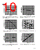
14 / 20 page  AD6432 –14– REV. 0 Local Oscillator Input The Local Oscillator (LO) input port is differential and consists of two functionally identical pins, LOHI and LOLO. It accepts a signal of 200 mV p-p at a frequency between 200 MHz and 600 MHz. Inputs LOHI and LOLO are internally biased to the positive supply (Pin 3) through 500 Ω resistors. While not usu- ally needed, these inputs may be driven through a simple match- ing network to lower the LO power required from a 50 Ω source. Single-sided drives are not recommended. The most noticeable effects will be degradation of phase balance and an increase in phase noise. This signal is fed internally to a divider by two that generates the mixing signals for the receive mixer and the transmit modulator. In order to meet the phase and amplitude balance of the trans- mit quadrature modulator, as stated in the specification table, the duty cycle of the LO signal must be such that the second harmonic is at least 30 dBc below the fundamental. I/Q Convention The AD6432 is a complete IF subsystem. Although not a re- quirement for using the AD6432, most applications will use a high side LO injection on the receive mixer. The I and Q con- vention on the receive section is such that when a spectrum with I leading Q is presented to the input of the receive mixer and a high side LO is presented to the receive mixer, I still leads Q at the baseband output of the AD6432. Likewise, the I and Q convention on the transmit section is such that when a spectrum with I leading Q is presented at the baseband input of the modulator, I still leads Q at the output of the modulator. Auxiliary Op Amp An auxiliary operational amplifier is available although it is im- portant to remember that it is active only when TXPU is high. The positive and negative input terminals are PCAP and PCAM with PCAO being the output pin. The inputs are the bases of PNP transistors with a typical bias current of approximately 150 nA. The input offset voltage is typically < 4 mV and the open loop gain of the amplifier is 60 dB. The amplifier is unity gain stable with a –3 dB Bandwidth greater than 40 MHz. The input signal voltage range is from 0.1 V to VPOS – 2.1 V. Bias System The AD6432 operates from a single supply, VPOS, usually 3 V, at a typical supply current in receive mode of 13 mA at midgain and TA = +25 °C, corresponding to a power consumption of 39 mW. Any voltage from 2.7 V to 3.6 V may be used. The bias system includes a fast-acting active high CMOS-com- patible power-up switch, allowing the part to idle at less than 100 µA when disabled. Biasing is generally proportional-to- absolute temperature (PTAT) to ensure stable gain with tem- perature. Other special biasing techniques are used to ensure very accurate gain, stable over the full temperature range. USING THE AD6432 In this section, we will focus on a few areas of special impor- tance through the real life example of interfacing the AD6432 to the AD6421 Base Band converter. As is true of any wideband high gain components, great care is needed in PC board layout. The location of the particular grounding points must be considered with due regard for the possibility of unwanted signal coupling. The high sensitivity of the AD6432 leads to the possibility that unwanted local EM signals may have an effect on the per- formance. During system development, carefully-shielded test assemblies should be used. The best solution is to use a fully enclosed box enclosing all components, with the minimum number of needed signal connectors (RF, LO, I and Q outputs) in miniature coax form. Interfacing the AD6432 to the AD6421 Baseband Converter The AD6421 Baseband Converter contains all the necessary elements to drive the AD6432. Receive Interface The interface between the two devices provides for quadrature I and Q channels that can be driven either differentially or in the single-ended configuration. Figure 35 shows the interface be- tween the AD6432 and the AD6421 for the differential configu- ration. The respective pins (IRXP, IRXN, QRXP and QRXN) are dc coupled through 4.7 k Ω resistors, which are integrated within the AD6432. Balanced coupling may be used with a single 50 pF capacitor between the complementary signals as illustrated in Figure 35. This low-pass filter is the only external filter required to prevent aliasing of the baseband analog signal prior to sampling within the AD6421. The AD6421 has an external autocalibration mode that can calibrate out any offsets resulting from the IF demodulation circuitry. Transmit Interface The corresponding transmit (ITXP, ITXN, QTXP and QTXN) pins of the AD6421 and AD6432 are directly connected as these have compatible bias levels for dc coupling. To meet the more stringent phase two filter mask requirements, an external low- pass filter may be required, depending on the filtering capabili- ties of the radio section. A passive second order low-pass filter network with a cutoff frequency to 600 kHz is suggested as shown in Figure 34. Resistor values should range from 1.5 k Ω–3.0 kΩ to minimize AD6432 offsets. QTXN QTXP ITXN ITXP AD6432 AD6421 ITXP ITXN QTXP QTXN Figure 34. GSM Phase II Transmit Interface |
|
|
링크 URL |
| ALLDATASHEET 가 귀하에 도움이 되셨나요? [ DONATE ] |
Alldatasheet는? | 광고문의 | 운영자에게 연락하기 | 개인정보취급방침 | 링크 투 데이터시트 | 링크교환 | 제조사별 검색 All Rights Reserved©Alldatasheet.com |
| Russian : Alldatasheetru.com | Korean : Alldatasheet.co.kr | Spanish : Alldatasheet.es | French : Alldatasheet.fr | Italian : Alldatasheetit.com Portuguese : Alldatasheetpt.com | Polish : Alldatasheet.pl | Vietnamese : Alldatasheet.vn Indian : Alldatasheet.in | Mexican : Alldatasheet.com.mx | British : Alldatasheet.co.uk | New Zealand : Alldatasheet.co.nz |
|
Family Site : ic2ic.com |
icmetro.com |
 Korean ▼
 English
 Chinese
 German
 Japanese
 Russian
 Korean
 Spanish
 French
 Italian
 Portuguese
 Polish
 Vietnamese
 Indian
 Mexican
 British
 New Zealand