|
전자부품 데이터시트 검색엔진 |
|
|
전자부품 데이터시트 검색엔진 |
|
CC1150-RTY1 데이터시트(PDF) 37 Page - Texas Instruments |
|
|
|||||||||||||||||||||||||||||
CC1150-RTY1 데이터시트(HTML) 37 Page - Texas Instruments |
|
|
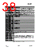
37 / 67 page  CC1150 SWRS037A Page 37 of 60 22 General Purpose / Test Output Control Pins The two digital output pins GDO0 and GDO1 are general control pins. Their functions are programmed by IOCFG0.GDO0_CFG and IOCFG1.GDO1_CFG respectively. Table 24 shows the different signals that can be monitored on the GDO pins. These signals can be used as an interrupt to the MCU. GDO1 is the same pin as the SO pin on the SPI interface, thus the output programmed on this pin will only be valid when CSn is high. The default value for GDO1 is 3-stated, which is useful when the SPI interface is shared with other devices. The default value for GDO0 is a 125 - 146 kHz clock output (XOSC frequency divided by 192). Since the XOSC is turned on at power- on-reset, this can be used to clock the MCU in systems with only one crystal. When the MCU is up and running it can change the clock frequency by writing to IOCFG0.GDO0_CFG. An on-chip analog temperature sensor is enabled by writing the value 128 (0x80h) to the IOCFG0.GDO0_CFG register. The voltage on the GDO0 pin is then proportional to temperature. See section 4.5 on page 9 for temperature sensor specifications. |
|
링크 URL |
| ALLDATASHEET 가 귀하에 도움이 되셨나요? [ DONATE ] |
Alldatasheet는? | 광고문의 | 운영자에게 연락하기 | 개인정보취급방침 | 링크 투 데이터시트 | 링크교환 | 제조사별 검색 All Rights Reserved©Alldatasheet.com |
| Russian : Alldatasheetru.com | Korean : Alldatasheet.co.kr | Spanish : Alldatasheet.es | French : Alldatasheet.fr | Italian : Alldatasheetit.com Portuguese : Alldatasheetpt.com | Polish : Alldatasheet.pl | Vietnamese : Alldatasheet.vn Indian : Alldatasheet.in | Mexican : Alldatasheet.com.mx | British : Alldatasheet.co.uk | New Zealand : Alldatasheet.co.nz |
|
Family Site : ic2ic.com |
icmetro.com |
 Korean ▼
 English
 Chinese
 German
 Japanese
 Russian
 Korean
 Spanish
 French
 Italian
 Portuguese
 Polish
 Vietnamese
 Indian
 Mexican
 British
 New Zealand