|
전자부품 데이터시트 검색엔진 |
|
|
전자부품 데이터시트 검색엔진 |
|
AS3930 데이터시트(PDF) 15 Page - ams AG |
|
|
|||||||||||||||||||||||||||||
AS3930 데이터시트(HTML) 15 Page - ams AG |
|
|
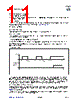
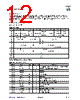
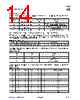
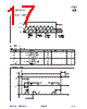
15 / 32 page  www.ams.com/LF-Receiver/AS3930 Revision 1.5 15 - 32 AS3930 Datasheet - Detailed Descr i p ti on The last 8 bits are the data that has to be written respectively read. A CS toggle high-low-high terminates the command mode. If a direct command is sent (B15-B14=11), then the bits from B13 to B8 define the direct command while the last 8 bits are omitted. Table 12 shows all possible direct commands. All direct commands are explained below: - clear_wake: Clears the wake state of the chip. In case the chip has woken up (WAKE pin is high), the chip is set back to listening mode. - reset_RSSI: Resets the RSSI measurement. - trim_osc: Starts the trimming procedure of the internal RC oscillator (see Figure 20). - clear_false: Resets the false wake-up register (R13<7:0>=00). - preset_default: Sets all registers in the default mode, as shown in Figure 7. Note: In order to get the AS3930 work properly after sending the preset_default direct command, it is mandatory to write R0<3>=0 and R0<2> =0. Writing of Data to Addressable Registers (WRITE Mode) The SDI is sampled at the falling edge of SCLK (as shown in the following diagrams). A CS toggling high-low-high indicates the end of the WRITE command after register has been written. The following example shows a write command. Figure 12. Writing of a Single Byte (falling edge sampling) 001 011 R11 001 100 R12 001 101 R13 Table 12. List of Direct Commands COMMAND_MODE B13 B12 B11 B10 B9 B8 clear_wake 0 0 0 0 0 0 reset_RSSI 0 0 0 0 0 1 trim_osc 0 000 1 0 clear_false 0 000 1 1 preset_default 0 0 0 1 0 0 Table 11. Bits B13-B8 B13 B12 B11 B10 B9 B8 Read/Write Register CS SCLK SDI 0 0 A5 A4 A3 A2 A1 A0 D5 D4 D3 D2 D1 D0 D7 D6 X X SCLK rising edge Data is transfered from µC SCLK falling edge Data is sampled Data is moved to Address A5-A0 CS falling edge signals end of WRITE Mode Two leading Zeros indicate WRITE Mode |
|
링크 URL |
| ALLDATASHEET 가 귀하에 도움이 되셨나요? [ DONATE ] |
Alldatasheet는? | 광고문의 | 운영자에게 연락하기 | 개인정보취급방침 | 링크 투 데이터시트 | 링크교환 | 제조사별 검색 All Rights Reserved©Alldatasheet.com |
| Russian : Alldatasheetru.com | Korean : Alldatasheet.co.kr | Spanish : Alldatasheet.es | French : Alldatasheet.fr | Italian : Alldatasheetit.com Portuguese : Alldatasheetpt.com | Polish : Alldatasheet.pl | Vietnamese : Alldatasheet.vn Indian : Alldatasheet.in | Mexican : Alldatasheet.com.mx | British : Alldatasheet.co.uk | New Zealand : Alldatasheet.co.nz |
|
Family Site : ic2ic.com |
icmetro.com |
 Korean ▼
 English
 Chinese
 German
 Japanese
 Russian
 Korean
 Spanish
 French
 Italian
 Portuguese
 Polish
 Vietnamese
 Indian
 Mexican
 British
 New Zealand