|
전자부품 데이터시트 검색엔진 |
|
|
전자부품 데이터시트 검색엔진 |
|
IS25LP256-RMLA 데이터시트(PDF) 7 Page - Integrated Silicon Solution, Inc |
|
|
|||||||||||||||||||||||||||||
IS25LP256-RMLA 데이터시트(HTML) 7 Page - Integrated Silicon Solution, Inc |
|
|
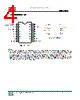
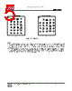
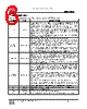
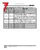
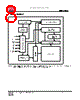
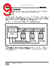
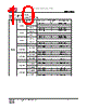
7 / 15 page  IS25LP256 Integrated Silicon Solution, Inc.- www.issi.com 7 Rev.00A 1/16/2014 For 16-pin SOIC 300mil package with additional RESET# pin option - RESET# pin will be added to another pin without sharing with HOLD# pin (Call Factory for the parts) SYMBOL TYPE DESCRIPTION CE# INPUT Same as the description in previous page SI (IO0), SO (IO1) INPUT/OUTPUT Same as the description in previous page WP# (IO2) INPUT/OUTPUT Same as the description in previous page HOLD# (IO3) INPUT/OUTPUT HOLD#/Serial Data IO (IO3): When the QE bit of Status Register is set to “1”, HOLD# pin is not available since it becomes IO3. When QE=0 the pin acts as HOLD# regardless of the P7 bit of Read Register. The HOLD# pin allows the device to be paused while it is selected. It pauses serial communication by the master device without resetting the serial sequence. The HOLD# pin is active low. When HOLD# is in a low state and CE# is low, the SO pin will be at high impedance. Device operation can resume when HOLD# pin is brought to a high state. RESET# INPUT/OUTPUT RESET: This pin is available only for dedicated parts (Call Factory). The RESET# pin is a hardware RESET signal. When RESET# is driven HIGH, the memory is in the normal operating mode. When RESET# is driven LOW, the memory enters reset mode and output is High-Z. If RESET# is driven LOW while an internal WRITE, PROGRAM, or ERASE operation is in progress, data may be lost. SCK INPUT Same as the description in previous page Vcc POWER Same as the description in previous page GND GROUND Same as the description in previous page NC Unused Same as the description in previous page ADVANCED INFORMATION |
|
|
링크 URL |
| ALLDATASHEET 가 귀하에 도움이 되셨나요? [ DONATE ] |
Alldatasheet는? | 광고문의 | 운영자에게 연락하기 | 개인정보취급방침 | 링크 투 데이터시트 | 링크교환 | 제조사별 검색 All Rights Reserved©Alldatasheet.com |
| Russian : Alldatasheetru.com | Korean : Alldatasheet.co.kr | Spanish : Alldatasheet.es | French : Alldatasheet.fr | Italian : Alldatasheetit.com Portuguese : Alldatasheetpt.com | Polish : Alldatasheet.pl | Vietnamese : Alldatasheet.vn Indian : Alldatasheet.in | Mexican : Alldatasheet.com.mx | British : Alldatasheet.co.uk | New Zealand : Alldatasheet.co.nz |
|
Family Site : ic2ic.com |
icmetro.com |
 Korean ▼
 English
 Chinese
 German
 Japanese
 Russian
 Korean
 Spanish
 French
 Italian
 Portuguese
 Polish
 Vietnamese
 Indian
 Mexican
 British
 New Zealand