|
전자부품 데이터시트 검색엔진 |
|
|
전자부품 데이터시트 검색엔진 |
|
IS25LP256-RMLA 데이터시트(PDF) 9 Page - Integrated Silicon Solution, Inc |
|
|
|||||||||||||||||||||||||||||
IS25LP256-RMLA 데이터시트(HTML) 9 Page - Integrated Silicon Solution, Inc |
|
|
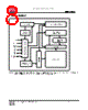
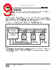
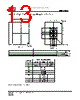
9 / 15 page  IS25LP256 Integrated Silicon Solution, Inc.- www.issi.com 9 Rev.00A 1/16/2014 SPI MODES DESCRIPTION Multiple IS25LP256 devices can be connected on the SPI serial bus and controlled by a SPI Master, i.e. microcontroller, as shown in Figure 4.1. The devices support either of two SPI modes: Mode 0 (0, 0) Mode 3 (1, 1) The difference between these two modes is the clock polarity. When the SPI master is in stand-by mode, the serial clock remains at “0” (SCK = 0) for Mode 0 and the clock remains at “1” (SCK = 1) for Mode 3. Please refer to Figure 4.2 and Figure 4.3 for SPI and QPI mode. In both modes, the input data is latched on the rising edge of Serial Clock (SCK), and the output data is available from the falling edge of SCK. Figure 4.1 Connection Diagram among SPI Master and SPI Slaves (Memory Devices) Notes: 1. In case of 16-pin SOIC package, RESET# pin will be added to another pin without sharing with HOLD# pin for the dedicated parts. Call Factory for the additional RESET# pin option. 2. SI and SO pins become bidirectional IO0 and IO1, and WP# and HOLD# pins become IO2 and IO3 respectively during QPI mode. SPI interface with (0,0) or (1,1) SPI Master (i.e. Microcontroller) SPI Memory Device SPI Memory Device SPI Memory Device SCK SO SI SCK SDI SDO CE# WP# HOLD# or RESET SCK SO SI CE# WP# HOLD# or RESET# SCK SO SI CE# WP# CS3 CS2 CS1 HOLD# or RESET# (1) (1) (1) ADVANCED INFORMATION |
|
|
링크 URL |
| ALLDATASHEET 가 귀하에 도움이 되셨나요? [ DONATE ] |
Alldatasheet는? | 광고문의 | 운영자에게 연락하기 | 개인정보취급방침 | 링크 투 데이터시트 | 링크교환 | 제조사별 검색 All Rights Reserved©Alldatasheet.com |
| Russian : Alldatasheetru.com | Korean : Alldatasheet.co.kr | Spanish : Alldatasheet.es | French : Alldatasheet.fr | Italian : Alldatasheetit.com Portuguese : Alldatasheetpt.com | Polish : Alldatasheet.pl | Vietnamese : Alldatasheet.vn Indian : Alldatasheet.in | Mexican : Alldatasheet.com.mx | British : Alldatasheet.co.uk | New Zealand : Alldatasheet.co.nz |
|
Family Site : ic2ic.com |
icmetro.com |
 Korean ▼
 English
 Chinese
 German
 Japanese
 Russian
 Korean
 Spanish
 French
 Italian
 Portuguese
 Polish
 Vietnamese
 Indian
 Mexican
 British
 New Zealand