|
전자부품 데이터시트 검색엔진 |
|
|
전자부품 데이터시트 검색엔진 |
|
ADC12H030 데이터시트(PDF) 11 Page - National Semiconductor (TI) |
|
|
|
|||||||||||||||||||||||||||||
ADC12H030 데이터시트(HTML) 11 Page - National Semiconductor (TI) |
|
|
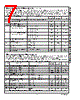
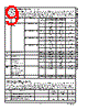
11 / 41 page  Note 5: The human body model is a 100 pF capacitor discharged through a 1.5 k Ω resistor into each pin. Note 6: See AN450 “Surface Mounting Methods and Their Effect on Product Reliability” or the section titled “Surface Mount” found in any post 1986 National Semiconductor Linear Data Book for other methods of soldering surface mount devices. Note 7: Two on-chip diodes are tied to each analog input through a series resistor as shown below. Input voltage magnitude up to 5V above VA+ or 5V below GND will not damage this device. However, errors in the A/D conversion can occur (if these diodes are forward biased by more than 50 mV) if the input voltage magnitude of selected or unselected analog input go above VA+ or below GND by more than 50 mV. As an example, if VA+ is 4.5 VDC, full-scale input voltage must be ≤4.55 VDC to ensure accurate conversions. 01135402 Note 8: To guarantee accuracy, it is required that the VA+ and VD+ be connected together to the same power supply with separate bypass capacitors at each V + pin. Note 9: With the test condition for VREF (VREF+−VREF−) given as +4.096V, the 12-bit LSB is 1.0 mV and the 8-bit LSB is 16.0 mV. Note 10: Typicals are at TJ =TA = 25˚C and represent most likely parametric norm. Note 11: Tested limits are guaranteed to National’s AOQL (Average Outgoing Quality Level). Note 12: Positive integral linearity error is defined as the deviation of the analog value, expressed in LSBs, from the straight line that passes through positive full-scale and zero. For negative integral linearity error, the straight line passes through negative full-scale and zero (see Figures 2, 3). Note 13: Zero error is a measure of the deviation from the mid-scale voltage (a code of zero), expressed in LSB. It is the worst-case value of the code transitions between 1 to 0 and 0 to +1 (see Figure 4). Note 14: Total unadjusted error includes offset, full-scale, linearity and multiplexer errors. Note 15: The DC common-mode error is measured in the differential multiplexer mode with the assigned positive and negative input channels shorted together. Note 16: Channel leakage current is measured after the channel selection. Note 17: Timing specifications are tested at the TTL logic levels, VIL = 0.4V for a falling edge and VIH = 2.4V for a rising edge. TRI-STATE output voltage is forced to 1.4V. Note 18: The ADC12030 family’s self-calibration technique ensures linearity and offset errors as specified, but noise inherent in the self-calibration process will result in a maximum repeatability uncertainty of 0.2 LSB. Note 19: If SCLK and CCLK are driven from the same clock source, then tA is 6, 10, 18 or 34 clock periods minimum and maximum. Note 20: The “12-Bit Conversion of Offset” and “12-Bit Conversion of Full-Scale” modes are intended to test the functionality of the device. Therefore, the output data from these modes are not an indication of the accuracy of a conversion result. 01135410 FIGURE 1. Transfer Characteristic www.national.com 11 |
|
링크 URL |
| ALLDATASHEET 가 귀하에 도움이 되셨나요? [ DONATE ] |
Alldatasheet는? | 광고문의 | 운영자에게 연락하기 | 개인정보취급방침 | 링크 투 데이터시트 | 링크교환 | 제조사별 검색 All Rights Reserved©Alldatasheet.com |
| Russian : Alldatasheetru.com | Korean : Alldatasheet.co.kr | Spanish : Alldatasheet.es | French : Alldatasheet.fr | Italian : Alldatasheetit.com Portuguese : Alldatasheetpt.com | Polish : Alldatasheet.pl | Vietnamese : Alldatasheet.vn Indian : Alldatasheet.in | Mexican : Alldatasheet.com.mx | British : Alldatasheet.co.uk | New Zealand : Alldatasheet.co.nz |
|
Family Site : ic2ic.com |
icmetro.com |
 Korean ▼
 English
 Chinese
 German
 Japanese
 Russian
 Korean
 Spanish
 French
 Italian
 Portuguese
 Polish
 Vietnamese
 Indian
 Mexican
 British
 New Zealand