|
전자부품 데이터시트 검색엔진 |
|
|
전자부품 데이터시트 검색엔진 |
|
CC1100-RTY1 데이터시트(PDF) 18 Page - Texas Instruments |
|
|
|
|||||||||||||||||||||||||||||
CC1100-RTY1 데이터시트(HTML) 18 Page - Texas Instruments |
|
|
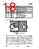
18 / 100 page  CC1100 SWRS038D Page 18 of 92 Pin # Pin Name Pin type Description 11 AVDD Power (Analog) 1.8 -3.6 V analog power supply connection 12 RF_P RF I/O Positive RF input signal to LNA in receive mode Positive RF output signal from PA in transmit mode 13 RF_N RF I/O Negative RF input signal to LNA in receive mode Negative RF output signal from PA in transmit mode 14 AVDD Power (Analog) 1.8 - 3.6 V analog power supply connection 15 AVDD Power (Analog) 1.8 - 3.6 V analog power supply connection 16 GND Ground (Analog) Analog ground connection 17 RBIAS Analog I/O External bias resistor for reference current 18 DGUARD Power (Digital) Power supply connection for digital noise isolation 19 GND Ground (Digital) Ground connection for digital noise isolation 20 SI Digital Input Serial configuration interface, data input Table 13: Pinout Overview 6 Circuit Description BIAS PA RBIAS XOSC_Q1 XOSC_Q2 CSn SI SO (GDO1) XOSC SCLK LNA 0 90 FREQ SYNTH ADC ADC RADIO CONTROL RF_P RF_N GDO2 GDO0 (ATEST) RC OSC Figure 2: CC1100 Simplified Block Diagram A simplified block diagram of CC1100 is shown in Figure 2. CC1100 features a low-IF receiver. The received RF signal is amplified by the low- noise amplifier (LNA) and down-converted in quadrature (I and Q) to the intermediate frequency (IF). At IF, the I/Q signals are digitised by the ADCs. Automatic gain control (AGC), fine channel filtering and demodulation bit/packet synchronization are performed digitally. The transmitter part of CC1100 is based on direct synthesis of the RF frequency. The frequency synthesizer includes a completely on-chip LC VCO and a 90 degree phase shifter for generating the I and Q LO signals to the down-conversion mixers in receive mode. A crystal is to be connected to XOSC_Q1 and XOSC_Q2. The crystal oscillator generates the reference frequency for the synthesizer, as well as clocks for the ADC and the digital part. A 4-wire SPI serial interface is used for configuration and data buffer access. The digital baseband includes support for channel configuration, packet handling, and data buffering. |
|
링크 URL |
| ALLDATASHEET 가 귀하에 도움이 되셨나요? [ DONATE ] |
Alldatasheet는? | 광고문의 | 운영자에게 연락하기 | 개인정보취급방침 | 링크 투 데이터시트 | 링크교환 | 제조사별 검색 All Rights Reserved©Alldatasheet.com |
| Russian : Alldatasheetru.com | Korean : Alldatasheet.co.kr | Spanish : Alldatasheet.es | French : Alldatasheet.fr | Italian : Alldatasheetit.com Portuguese : Alldatasheetpt.com | Polish : Alldatasheet.pl | Vietnamese : Alldatasheet.vn Indian : Alldatasheet.in | Mexican : Alldatasheet.com.mx | British : Alldatasheet.co.uk | New Zealand : Alldatasheet.co.nz |
|
Family Site : ic2ic.com |
icmetro.com |
 Korean ▼
 English
 Chinese
 German
 Japanese
 Russian
 Korean
 Spanish
 French
 Italian
 Portuguese
 Polish
 Vietnamese
 Indian
 Mexican
 British
 New Zealand