|
전자부품 데이터시트 검색엔진 |
|
|
전자부품 데이터시트 검색엔진 |
|
T89C5115-RATIM 데이터시트(PDF) 30 Page - ATMEL Corporation |
|
|
|||||||||||||||||||||||||||||
T89C5115-RATIM 데이터시트(HTML) 30 Page - ATMEL Corporation |
|
|
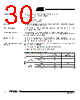
30 / 105 page  30 T89C5115 4128A–8051–04/02 FM0 Memory Architecture The Flash memory is made up of 4 blocks (see Figure 11): 1. The memory array (user space) 16-KB. 2. The Extra Row. 3. The Hardware security bits. 4. The column latch registers. User Space This space is composed of a 16-KB Flash memory organized in 128 pages of 128 bytes. It contains the user’s application code. Extra Row (XROW) This row is a part of FM0 and has a size of 128 bytes. The extra row may contain infor- mation for boot loader usage. Hardware security Byte The Hardware Security Byte space is a part of FM0 and has a size of 1 byte. The 4 MSB can be read/written by software, the 4 LSB can only be read by software and written by hardware in parallel mode. Column Latches The column latches, also part of FM0, have a size of full page (128 bytes). The column latches are the entrance buffers of the three previous memory locations (user array, XROW and Hardware security byte). Cross Flash Memory Access Description The FM0 memory can be program only from FM1. Programming FM0 from FM0 or from external memory is impossible. The FM1 memory can be program only by parallel programming. The Table 19 show all software flash access allowed. Table 19. Cross Flash Memory Access Action FM0 (user Flash) FM1 (boot Flash) FM0 (user Flash) Read ok - Load column latch ok - Write - - FM1 (boot flash) Read ok ok Load column latch ok - Write ok - |
|
링크 URL |
| ALLDATASHEET 가 귀하에 도움이 되셨나요? [ DONATE ] |
Alldatasheet는? | 광고문의 | 운영자에게 연락하기 | 개인정보취급방침 | 링크 투 데이터시트 | 링크교환 | 제조사별 검색 All Rights Reserved©Alldatasheet.com |
| Russian : Alldatasheetru.com | Korean : Alldatasheet.co.kr | Spanish : Alldatasheet.es | French : Alldatasheet.fr | Italian : Alldatasheetit.com Portuguese : Alldatasheetpt.com | Polish : Alldatasheet.pl | Vietnamese : Alldatasheet.vn Indian : Alldatasheet.in | Mexican : Alldatasheet.com.mx | British : Alldatasheet.co.uk | New Zealand : Alldatasheet.co.nz |
|
Family Site : ic2ic.com |
icmetro.com |
 Korean ▼
 English
 Chinese
 German
 Japanese
 Russian
 Korean
 Spanish
 French
 Italian
 Portuguese
 Polish
 Vietnamese
 Indian
 Mexican
 British
 New Zealand