|
전자부품 데이터시트 검색엔진 |
|
|
전자부품 데이터시트 검색엔진 |
|
AL5802 데이터시트(PDF) 2 Page - Diodes Incorporated |
|
|
|||||||||||||||||||||||||||||
AL5802 데이터시트(HTML) 2 Page - Diodes Incorporated |
|
|
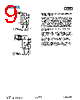
2 / 11 page  AL5802 Document number: DS35516 Rev. 9 - 2 2 of 11 www.diodes.com March 2014 © Diodes Incorporated AL5802 Pin Descriptions Pin Number Name Function 1 OUT Open-collector LED driver output 2 BIAS Biases the open collector output transistor 3 EN Enable pin for PWM dimming. Provides access to the base of Q2 and collector of Q1 4 GND Ground reference point for setting LED current 5 FB Feedback pin. Should be connected to pin 6. 6 REXT Current sense pin. LED current sensing resistor should be connected from here to GND. Functional Block Diagram Fig. 1 Block Diagram Absolute Maximum Ratings Symbol Characteristics Values Unit VOUT Output voltage relative to GND 30 V VBIAS BIAS voltage relative to GND (Note 4) 30 V VFB LED voltage relative to GND 6 V VEN EN voltage relative to GND 6 V VREXT REXT voltage relative to GND 6 V IOUT Output current 150 mA TJ Operating junction temperature -40 to +150 °C TST Storage temperature -55 to +150 °C These are stress ratings only. Operation outside the absolute maximum ratings may cause device failure. Operation at the absolute maximum rating for extended periods may reduce device reliability. Note: 4. With pins 5 and 6 connected together. |
|
|
링크 URL |
| ALLDATASHEET 가 귀하에 도움이 되셨나요? [ DONATE ] |
Alldatasheet는? | 광고문의 | 운영자에게 연락하기 | 개인정보취급방침 | 링크 투 데이터시트 | 링크교환 | 제조사별 검색 All Rights Reserved©Alldatasheet.com |
| Russian : Alldatasheetru.com | Korean : Alldatasheet.co.kr | Spanish : Alldatasheet.es | French : Alldatasheet.fr | Italian : Alldatasheetit.com Portuguese : Alldatasheetpt.com | Polish : Alldatasheet.pl | Vietnamese : Alldatasheet.vn Indian : Alldatasheet.in | Mexican : Alldatasheet.com.mx | British : Alldatasheet.co.uk | New Zealand : Alldatasheet.co.nz |
|
Family Site : ic2ic.com |
icmetro.com |
 Korean ▼
 English
 Chinese
 German
 Japanese
 Russian
 Korean
 Spanish
 French
 Italian
 Portuguese
 Polish
 Vietnamese
 Indian
 Mexican
 British
 New Zealand