|
전자부품 데이터시트 검색엔진 |
|
|
전자부품 데이터시트 검색엔진 |
|
ADL5369ACPZ-R7 데이터시트(PDF) 18 Page - Analog Devices |
|
|
|||||||||||||||||||||||||||||
ADL5369ACPZ-R7 데이터시트(HTML) 18 Page - Analog Devices |
|
|
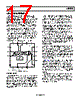
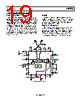
18 / 23 page  ADL5369 Data Sheet Rev. A | Page 18 of 23 The performance of this amplifier is critical in achieving a high intercept passive mixer without degrading the noise floor of the system. This is a critical requirement in an interferer rich environment, such as cellular infrastructure, where blocking interferers can limit mixer performance. The bandwidth of the intermodulation performance is somewhat influenced by the current in the LO amplifier chain. For dc current sensitive applications, it is permissible to reduce the current in the LO amplifier by raising the value of the external bias control resistor. For dc current critical applications, the LO chain can operate with a supply voltage as low as 3.3 V, resulting in substantial dc power savings. In addition, when operating with supply voltages below 3.6 V, the ADL5369 has a power-down mode that permits the dc current to drop to <200 μA. All of the logic inputs work with any logic family that provides a Logic 0 input level of less than 0.4 V and a Logic 1 input level that exceeds 1.4 V. All logic inputs are high impedance up to Logic 1 levels of 3.3 V. At levels exceeding 3.3 V, protection circuitry permits operation up to 5.5 V, although a small bias current is drawn. |
|
|
링크 URL |
| ALLDATASHEET 가 귀하에 도움이 되셨나요? [ DONATE ] |
Alldatasheet는? | 광고문의 | 운영자에게 연락하기 | 개인정보취급방침 | 링크 투 데이터시트 | 링크교환 | 제조사별 검색 All Rights Reserved©Alldatasheet.com |
| Russian : Alldatasheetru.com | Korean : Alldatasheet.co.kr | Spanish : Alldatasheet.es | French : Alldatasheet.fr | Italian : Alldatasheetit.com Portuguese : Alldatasheetpt.com | Polish : Alldatasheet.pl | Vietnamese : Alldatasheet.vn Indian : Alldatasheet.in | Mexican : Alldatasheet.com.mx | British : Alldatasheet.co.uk | New Zealand : Alldatasheet.co.nz |
|
Family Site : ic2ic.com |
icmetro.com |
 Korean ▼
 English
 Chinese
 German
 Japanese
 Russian
 Korean
 Spanish
 French
 Italian
 Portuguese
 Polish
 Vietnamese
 Indian
 Mexican
 British
 New Zealand