|
전자부품 데이터시트 검색엔진 |
|
|
전자부품 데이터시트 검색엔진 |
|
AD9959/PCBZ 데이터시트(PDF) 36 Page - Analog Devices |
|
|
|||||||||||||||||||||||||||||
AD9959/PCBZ 데이터시트(HTML) 36 Page - Analog Devices |
|
|
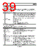
36 / 44 page  AD9959 Data Sheet Rev. C | Page 36 of 44 REGISTER MAPS AND BIT DESCRIPTIONS REGISTER MAPS Table 28. Control Register Map Register Name (Serial Address) Bit Range Bit 7 (MSB) Bit 6 Bit 5 Bit 4 Bit 3 Bit 2 Bit 1 Bit 0 (LSB) Default Value Channel Select Register (CSR) (0x00) [7:0] Channel 3 enable1 Channel 2 enable1 Channel 1 enable1 Channel 0 enable1 Must be 0 Serial I/O mode select[2:1] LSB first 0xF0 Function Register 1 (FR1) (0x01) [23:16] VCO gain control PLL divider ratio[22:18] Charge pump control[17:16] 0x00 [15:8] Open Profile pin configuration (PPC)[14:12] Ramp-up/ ramp-down (RU/RD)[11:10] Modulation level[9:8] 0x00 [7:0] Reference clock input power-down External power- down mode SYNC_CLK disable DAC reference power-down Open[3:2] Manual hardware sync Manual software sync 0x00 Function Register 2 (FR2) (0x02) [15:8] All channels autoclear sweep accumulator All channels clear sweep accumulator All channels autoclear phase accumulator All channels clear phase accumulator Open[11:10] Open[9:8] 0x00 [7:0] Auto sync enable Multidevice sync master enable Multidevice sync status Multidevice sync mask Open[3:2] System clock offset[1:0] 0x00 1 Channel enable bits do not require an I/O update to be activated. These bits are active immediately after the byte containing the bits is written. All other bits need an I/O update to become active. The four channel enable bits shown in Table 28 are used to enable/disable any combination of the four channels. The default for all four channels is enabled. In the channel select register, if the user wants four different frequencies for all four DDS channels, use the following protocol: 1. Enable (Logic 1) the Channel 0 enable bit, which is located in the channel select register, and disable the other three channels (Logic 0). 2. Write the desired frequency tuning word for Channel 0, as described in Step 1, and then disable the Channel 0 enable bit (Logic 0). 3. Enable the Channel 1 enable bit only, located in the channel select register, and disable the other three channels. 4. Write the desired frequency tuning word for Channel 1 in Step 3, then disable the Channel 1 enable bit. |
|
링크 URL |
| ALLDATASHEET 가 귀하에 도움이 되셨나요? [ DONATE ] |
Alldatasheet는? | 광고문의 | 운영자에게 연락하기 | 개인정보취급방침 | 링크 투 데이터시트 | 링크교환 | 제조사별 검색 All Rights Reserved©Alldatasheet.com |
| Russian : Alldatasheetru.com | Korean : Alldatasheet.co.kr | Spanish : Alldatasheet.es | French : Alldatasheet.fr | Italian : Alldatasheetit.com Portuguese : Alldatasheetpt.com | Polish : Alldatasheet.pl | Vietnamese : Alldatasheet.vn Indian : Alldatasheet.in | Mexican : Alldatasheet.com.mx | British : Alldatasheet.co.uk | New Zealand : Alldatasheet.co.nz |
|
Family Site : ic2ic.com |
icmetro.com |
 Korean ▼
 English
 Chinese
 German
 Japanese
 Russian
 Korean
 Spanish
 French
 Italian
 Portuguese
 Polish
 Vietnamese
 Indian
 Mexican
 British
 New Zealand