|
전자부품 데이터시트 검색엔진 |
|
|
전자부품 데이터시트 검색엔진 |
|
AD9959/PCBZ 데이터시트(PDF) 37 Page - Analog Devices |
|
|
|||||||||||||||||||||||||||||
AD9959/PCBZ 데이터시트(HTML) 37 Page - Analog Devices |
|
|
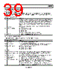
37 / 44 page  Data Sheet AD9959 Rev. C | Page 37 of 44 Table 29. Channel Register Map Register Name (Serial Address) Bit Range Bit 7 (MSB) Bit 6 Bit 5 Bit 4 Bit 3 Bit 2 Bit 1 Bit 0 (LSB) Default Value Channel Function Register1 (CFR) (0x03) [23:16] Amplitude freq. phase (AFP) select[23:22] Open[21:16] 0x00 [15:8] Linear sweep no-dwell Linear sweep enable Load SRR at I/O_UPDATE Open[12:11] Must be 0 DAC full-scale current control[9:8] 0x03 [7:0] Digital power- down DAC power- down Matched pipe delays active Autoclear sweep accumulator Clear sweep accumulator Autoclear phase accumulator Clear phase accumulator2 Sine wave output enable 0x02 Channel Frequency Tuning Word 01 (CFTW0) (0x04) [31:24] Frequency Tuning Word 0[31:24] 0x00 [23:16] Frequency Tuning Word 0[23:16] N/A [15:8] Frequency Tuning Word 0[15:8] N/A [7:0] Frequency Tuning Word 0[7:0] N/A Channel Phase Offset Word 01 (CPOW0) (0x05) [15:8] Open[15:14] Phase Offset Word 0[13:8] 0x00 [7:0] Phase Offset Word 0[7:0] 0x00 Amplitude Control Register (ACR) (0x06) [23:16] Amplitude ramp rate[23:16] N/A [15:8] Increment/decrement step size[15:14] Open Amplitude multiplier enable Ramp-up/ ramp-down enable Load ARR at I/O_UPDATE Amplitude scale factor[9:8] 0x00 [7:0] Amplitude scale factor[7:0] 0x00 Linear Sweep Ramp Rate1 (LSRR) (0x07) [15:8] Falling sweep ramp rate (FSRR)[15:8] N/A [7:0] Rising sweep ramp rate (RSRR)[7:0] N/A LSR Rising Delta Word1 (RDW) (0x08) [31:24] Rising delta word[31:24] N/A [23:16] Rising delta word[23:16] N/A [15:8] Rising delta word[15:8] N/A [7:0] Rising delta word[7:0] N/A LSR Falling Delta Word1 (FDW) (0x09) [31:24] Falling delta word[31:24] N/A [23:16] Falling delta word[23:16] N/A [15:8] Falling delta word[15:8] N/A [7:0] Falling delta word[7:0] N/A 1 There are four sets of channel registers and profile registers, one per channel. This is not shown in the Table 29 or Table 30 because the addresses of all channel registers and profile registers are the same for each channel. Therefore, the channel enable bits (CSR[7:4]) determine if the channel registers and/or profile registers of each channel are written to or not. 2 The clear phase accumulator bit is set to Logic 1 after a master reset. It self-clears or is set to Logic 0 when an I/O update is asserted. |
|
링크 URL |
| ALLDATASHEET 가 귀하에 도움이 되셨나요? [ DONATE ] |
Alldatasheet는? | 광고문의 | 운영자에게 연락하기 | 개인정보취급방침 | 링크 투 데이터시트 | 링크교환 | 제조사별 검색 All Rights Reserved©Alldatasheet.com |
| Russian : Alldatasheetru.com | Korean : Alldatasheet.co.kr | Spanish : Alldatasheet.es | French : Alldatasheet.fr | Italian : Alldatasheetit.com Portuguese : Alldatasheetpt.com | Polish : Alldatasheet.pl | Vietnamese : Alldatasheet.vn Indian : Alldatasheet.in | Mexican : Alldatasheet.com.mx | British : Alldatasheet.co.uk | New Zealand : Alldatasheet.co.nz |
|
Family Site : ic2ic.com |
icmetro.com |
 Korean ▼
 English
 Chinese
 German
 Japanese
 Russian
 Korean
 Spanish
 French
 Italian
 Portuguese
 Polish
 Vietnamese
 Indian
 Mexican
 British
 New Zealand