|
전자부품 데이터시트 검색엔진 |
|
|
전자부품 데이터시트 검색엔진 |
|
STM32U545NET3QTR 데이터시트(PDF) 139 Page - STMicroelectronics |
|
|
|||||||||||||||||||||||||||||
STM32U545NET3QTR 데이터시트(HTML) 139 Page - STMicroelectronics |
|
|
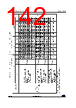
139 / 283 page  DS14216 Rev 1 139/283 STM32U545xx Electrical characteristics 258 5.3.4 Embedded voltage reference The parameters given in the table below are derived from tests performed under the ambient temperature and supply voltage conditions summarized in Table 33. tVBAT_BOR _sampling VBAT BOR sampling period in VBAT mode MONEN = 0(5) -0.5 2.5 s VAVM1 VDDA voltage monitor 1 threshold Rising edge 1.61 1.68 1.75 V Falling edge 1.58 1.65 1.71 VAVM2 VDDA voltage monitor 2 threshold Rising edge 1.77 1.86 1.95 Falling edge 1.73 1.82 1.9 VIO2VM VDDIO2 voltage monitor threshold - 0.96 1.01 1.05 VUVM VDDUSB voltage monitor threshold - 1.15 1.22 1.28 Vhyst_AVM Hysteresis of VDDA voltage monitor -- 40 - mV IDD_VM(2) Voltage monitor consumption from VDD (AVM1, AVM2, IO2VM or UVM single instance) -- 0.4 0.6 µA IDD_AVM_A(2) VDDA voltage monitor consumption from VDDA (resistor bridge) - - 1.25 1.85 1. Evaluated by characterization and not tested in production, unless otherwise specified. 2. Specified by design. Not tested in production 3. BOR0 is enabled in all modes (except Shutdown), and its consumption is therefore included in the supply current characteristics tables. 4. This is also the consumption saved in Standby mode when ULPMEN = 1. 5. VBAT brownout reset monitoring is discontinuous when MONEN = 0 in PWR_BDCR1, and is continuous when MONEN = 1. Table 35. Embedded reset and power control block characteristics(1) (continued) Symbol Parameter Conditions Min Typ Max Unit Table 36. Embedded internal voltage reference Symbol Parameter Conditions Min Typ Max Unit VREFINT(1) Internal reference voltage Range 1, 2, 3 1.175 1.215 1.255 V Range 4 and low-power modes 1.170 1.215 1.260 tS_vrefint(2)(3) ADC sampling time when reading the internal reference voltage - 12.65 - - µs tstart_vrefint(3) Start time of reference voltage buffer when the ADC is enabled -- 4 6 IDD(VREFINTBUF) (3) VREFINT buffer consumption from VDD when converted by the ADC - - 1.5 2.1 µA ∆VREFINT(4) Internal reference voltage spread over the temperature range VDD = 3 V - 6 11.5 mV TCoeff(4) Average temperature coefficient –40°C < TJ < +130 °C - 40 125 ppm/°C |
|
링크 URL |
| ALLDATASHEET 가 귀하에 도움이 되셨나요? [ DONATE ] |
Alldatasheet는? | 광고문의 | 운영자에게 연락하기 | 개인정보취급방침 | 링크 투 데이터시트 | 링크교환 | 제조사별 검색 All Rights Reserved©Alldatasheet.com |
| Russian : Alldatasheetru.com | Korean : Alldatasheet.co.kr | Spanish : Alldatasheet.es | French : Alldatasheet.fr | Italian : Alldatasheetit.com Portuguese : Alldatasheetpt.com | Polish : Alldatasheet.pl | Vietnamese : Alldatasheet.vn Indian : Alldatasheet.in | Mexican : Alldatasheet.com.mx | British : Alldatasheet.co.uk | New Zealand : Alldatasheet.co.nz |
|
Family Site : ic2ic.com |
icmetro.com |
 Korean ▼
 English
 Chinese
 German
 Japanese
 Russian
 Korean
 Spanish
 French
 Italian
 Portuguese
 Polish
 Vietnamese
 Indian
 Mexican
 British
 New Zealand