|
전자부품 데이터시트 검색엔진 |
|
|
전자부품 데이터시트 검색엔진 |
|
ISL97672 데이터시트(PDF) 3 Page - Renesas Technology Corp |
|
|
|||||||||||||||||||||||||||||
ISL97672 데이터시트(HTML) 3 Page - Renesas Technology Corp |
|
|
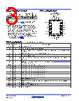
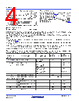
3 / 17 page  ISL97672 FN7632 Rev.4.00 Page 3 of 17 Sep 8, 2017 Pin Configuration ISL97672 (20 LD 4X3 QFN) TOP VIEW Ordering Information PART NUMBER (Notes 1, 2, 3) PART MARKING PACKAGE (RoHS Compliant) PKG. DWG. # ISL97672IRZ 7672 20 Ld 4x3 QFN L20.3x4 NOTES: 1. Add “-T” suffix for 6k unit or “-TK” suffix for 1k unit tape and reel options. Refer to TB347 for details on reel specifications. 2. These Intersil Pb-free plastic packaged products employ special Pb-free material sets, molding compounds/die attach materials, and 100% matte tin plate plus anneal (e3 termination finish, which is RoHS compliant and compatible with both SnPb and Pb-free soldering operations). Intersil Pb-free products are MSL classified at Pb-free peak reflow temperatures that meet or exceed the Pb-free requirements of IPC/JEDEC J STD-020. 3. For Moisture Sensitivity Level (MSL), please see device information page for ISL97672. For more information on MSL please see techbrief TB363. FAULT VIN EN VDC PWM /FLAG OVP CH5 CH4 CH3 CH2 CH1 1 2 3 4 5 6 16 15 14 13 12 11 20 19 18 17 789 10 Pin Descriptions (I = Input, O = Output, S = Supply) PIN NAME PIN # TYPE DESCRIPTION FAULT 1 O Fault disconnect switch VIN 2 S Input voltage for the device and LED power EN 3 I The device needs 4ms for initial power-up Enable. It will be disabled if it is not biased for longer than 28ms. VDC 4 S De-couple capacitor for internally generated supply rail. PWM 5 I PWM brightness control pin. /FLAG 6 O /Flag = 0 for any fault conditions. /Flag =1 for normal condition. Open drain that needs pull up. NC 7 I No Connect FSW 8 I Boost switching frequency set pin by connecting a resistor. See “Switching Frequency” on page 11 for resistor calculation AGND 9 S Analog Ground for precision circuits CH0 10 I Input 0 to current source, FB, and monitoring CH1 11 I Input 1 to current source, FB, and monitoring CH2 12 I Input 2 to current source, FB, and monitoring CH3 13 I Input 3 to current source, FB, and monitoring CH4 14 I Input 4 to current source, FB, and monitoring CH5 15 I Input 5 to current source, FB, and monitoring OVP 16 I Overvoltage protection input RSET 17 I Resistor connection for setting LED current, (see Equation 1 for calculating the ILEDpeak) COMP 18 O Boost compensation pin PGND 19 S Power ground (LX Power return) LX 20 O Input to boost switch |
|
|
링크 URL |
| ALLDATASHEET 가 귀하에 도움이 되셨나요? [ DONATE ] |
Alldatasheet는? | 광고문의 | 운영자에게 연락하기 | 개인정보취급방침 | 링크 투 데이터시트 | 링크교환 | 제조사별 검색 All Rights Reserved©Alldatasheet.com |
| Russian : Alldatasheetru.com | Korean : Alldatasheet.co.kr | Spanish : Alldatasheet.es | French : Alldatasheet.fr | Italian : Alldatasheetit.com Portuguese : Alldatasheetpt.com | Polish : Alldatasheet.pl | Vietnamese : Alldatasheet.vn Indian : Alldatasheet.in | Mexican : Alldatasheet.com.mx | British : Alldatasheet.co.uk | New Zealand : Alldatasheet.co.nz |
|
Family Site : ic2ic.com |
icmetro.com |
 Korean ▼
 English
 Chinese
 German
 Japanese
 Russian
 Korean
 Spanish
 French
 Italian
 Portuguese
 Polish
 Vietnamese
 Indian
 Mexican
 British
 New Zealand