|
전자부품 데이터시트 검색엔진 |
|
|
전자부품 데이터시트 검색엔진 |
|
ISL9222 데이터시트(PDF) 6 Page - Intersil Corporation |
|
|
|||||||||||||||||||||||||||||
ISL9222 데이터시트(HTML) 6 Page - Intersil Corporation |
|
|
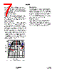
6 / 8 page  6 FN6643.1 March 10, 2008 input power is removed or the EN pin is pulled to HI. Figure 2 shows the typical charge waveforms after the power is on. A thermal foldback function reduces the charge current anytime when the die temperature reaches typically +115°C. This function guarantees safe operation when the printed-circuit board (PCB) is not capable of dissipating the heat generated by the linear charger. The ISL9222 accepts an input voltage up to 28V but disables charging when the input voltage exceeds the OVP threshold, typically 6.8V, to protect against unqualified or faulty AC adapters. PPR Indication The PPR pin is an open-drain output to indicate the presence of the ac adapter. Whenever the input voltage is higher than the POR threshold, the PPR pin turns on the internal open-drain MOSFET to indicate a logic LOW signal, independent on the EN pin input. When the internal open-drain FET is turned off, the PPR pin should leak less than 1µA current. When turned on, the PPR pin should be able to sink at least 10mA current under all operating conditions. The PPR pin can be used to drive an LED or to interface with a microprocessor. Power-Good Range The power-good range is defined by the following three conditions: 1. VIN > VPOR 2. VIN - VBAT > VOS 3. VIN < VOVP where VOS is the offset voltage for the input and output voltage comparator, discussed shortly, and VOVP is the overvoltage protection threshold given in the Electrical Specifications table on page 2. All VPOR, VOS, and VOVP have hysteresis, as given in the Electrical Specification table on page 2. The charger will not charge the battery if the input voltage is not in the power-good range. Input and Output Comparator The charger will not be enabled unless the input voltage is higher than the battery voltage by an offset voltage VOS. The purpose of this comparator is to ensure that the charger is turned off when the input power is removed from the charger. Without this comparator, it is possible that the charger will fail to power-down when the input is removed and the current can leak through the PFET pass element to continue biasing the POR and the Pre-Regulator blocks shown in the Block Diagram on page 5. EN Input EN is an active-low logic input to enable the charger. Drive the EN pin to LOW or leave it floating to enable the charger. This pin has a 200k Ω internal pulldown resistor so when left floating, the input is equivalent to logic LOW. Drive this pin to HIGH to disable the charger. The threshold for HIGH is given in the Electrical Specifications table on page 2. IREF Pin The IREF pin has the two functions as described in “Pin Descriptions” on page 3. When setting the fast charge current, the charge current is guaranteed to have 10% accuracy with the charge current set at 500mA. When monitoring the charge current, the accuracy of the IREF pin voltage vs. the actual charge current is the same as the gain from the IREF pin current to the actual charge current. The accuracy is 10% at 500mA and is expected to drop to 30% of the actual current (not the set constant charge current) when the current drops to 50mA. Operation Without the Battery The ISL9222 relies on a battery for stability and is not guaranteed to be stable if the battery is not connected. With a battery, the charger will be stable with an output ceramic decoupling capacitor in the range of 1µF to 200µF. The maximum load current is limited by the dropout voltage or the thermal foldback. Dropout Voltage The constant current may not be maintained due to the rDS(ON) limit at a low input voltage. The worst case ON-resistance of the pass FET is 1.2 Ω at the maximum operating temperature, thus if tested with 0.5A current and 3.8V battery voltage, constant current could not be maintained when the input voltage is below 4.4V. Thermal Foldback The thermal foldback function starts to reduce the charge current when the internal temperature reaches a typical value of +115°C. Auxiliary OR Gate The auxiliary OR gate provides a booting enable signal from from 2 possible inputs, the VIN power good signal, which is internal to the IC, or the external JIGIN signal. The supply voltage of the OR gate comes from VBAT. The JIGON states are summarized in Table 1. There is an internal pull-down resistor at the JIGIN pin so that when left floating, the input is a logic low. Applications Information Input Capacitor Selection The input capacitor is required to suppress the power supply transient response during transitions. Mainly, this capacitor is selected to avoid oscillation during the start up when the input supply is passing the POR threshold and the VIN-BAT comparator offset voltage. A 1µF or larger X5R ceramic capacitor is recommended. Due to the inductance of the power leads of the wall adapter or USB source, the input capacitor type must be properly selected to prevent high voltage transient during a hot-plug ISL9222 |
|
|
링크 URL |
| ALLDATASHEET 가 귀하에 도움이 되셨나요? [ DONATE ] |
Alldatasheet는? | 광고문의 | 운영자에게 연락하기 | 개인정보취급방침 | 링크 투 데이터시트 | 링크교환 | 제조사별 검색 All Rights Reserved©Alldatasheet.com |
| Russian : Alldatasheetru.com | Korean : Alldatasheet.co.kr | Spanish : Alldatasheet.es | French : Alldatasheet.fr | Italian : Alldatasheetit.com Portuguese : Alldatasheetpt.com | Polish : Alldatasheet.pl | Vietnamese : Alldatasheet.vn Indian : Alldatasheet.in | Mexican : Alldatasheet.com.mx | British : Alldatasheet.co.uk | New Zealand : Alldatasheet.co.nz |
|
Family Site : ic2ic.com |
icmetro.com |
 Korean ▼
 English
 Chinese
 German
 Japanese
 Russian
 Korean
 Spanish
 French
 Italian
 Portuguese
 Polish
 Vietnamese
 Indian
 Mexican
 British
 New Zealand