|
전자부품 데이터시트 검색엔진 |
|
|
전자부품 데이터시트 검색엔진 |
|
AT45DB021D 데이터시트(PDF) 21 Page - ATMEL Corporation |
|
|
|||||||||||||||||||||||||||||
AT45DB021D 데이터시트(HTML) 21 Page - ATMEL Corporation |
|
|
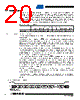
21 / 54 page  21 3638I–DFLASH–04/09 AT45DB021D 10.2.2 Reading the Security Register The Security Register can be read by first asserting the CS pin and then clocking in an opcode of 77H followed by three dummy bytes. After the last don’t care bit has been clocked in, the con- tent of the Security Register can be clocked out on the SO pins. After the last byte of the Security Register has been read, additional pulses on the SCK pin will simply result in undefined data being output on the SO pins. Deasserting the CS pin will terminate the Read Security Register operation and put the SO pins into a high-impedance state. Figure 10-4. Read Security Register 11. Additional Commands 11.1 Main Memory Page to Buffer Transfer A page of data can be transferred from the main memory to the buffer. To start the operation for the DataFlash standard page size (264 bytes), a 1-byte opcode, 53H, must be clocked into the device, followed by three address bytes comprised of 5 don’t care bits, 10 page address bits (PA9 - PA0), which specify the page in main memory that is to be transferred, and 9 don’t care bits. To perform a main memory page to buffer transfer for the binary page size (256 bytes), the opcode 53H must be clocked into the device followed by three address bytes consisting of 6 don’t care bits, 10 page address bits (A17 - A8) which specify the page in the main memory that is to be transferred, and 8 don’t care bits. The CS pin must be low while toggling the SCK pin to load the opcode and the address bytes from the input pin (SI). The transfer of the page of data from the main memory to the buffer will begin when the CS pin transitions from a low to a high state. During the transfer of a page of data (tXFR), the status register can be monitored to deter- mine whether the transfer has been completed. 11.2 Main Memory Page to Buffer Compare A page of data in main memory can be compared to the data in the buffer. To initiate the opera- tion for the DataFlash standard page size, a 1-byte opcode, 60H, must be clocked into the device, followed by three address bytes consisting of 5 don’t care bits, 10 page address bits (PA9 - PA0) that specify the page in the main memory that is to be compared to the buffer, and 9 don’t care bits. To start a main memory page to buffer compare for a binary page size, the opcode 60H must be clocked into the device followed by three address bytes consisting of 6 don’t care bits, 10 page address bits (A17 - A8) that specify the page in the main memory that is to be compared to the buffer, and 8 don’t care bits. The CS pin must be low while toggling the SCK pin to load the opcode and the address bytes from the input pin (SI). On the low-to-high transition of the CS pin, the data bytes in the selected main memory page will be compared with Opcode X X X Data Byte n Data Byte n + 1 CS Data Byte n + x Each transition represents 8 bits SI SO |
|
링크 URL |
| ALLDATASHEET 가 귀하에 도움이 되셨나요? [ DONATE ] |
Alldatasheet는? | 광고문의 | 운영자에게 연락하기 | 개인정보취급방침 | 링크 투 데이터시트 | 링크교환 | 제조사별 검색 All Rights Reserved©Alldatasheet.com |
| Russian : Alldatasheetru.com | Korean : Alldatasheet.co.kr | Spanish : Alldatasheet.es | French : Alldatasheet.fr | Italian : Alldatasheetit.com Portuguese : Alldatasheetpt.com | Polish : Alldatasheet.pl | Vietnamese : Alldatasheet.vn Indian : Alldatasheet.in | Mexican : Alldatasheet.com.mx | British : Alldatasheet.co.uk | New Zealand : Alldatasheet.co.nz |
|
Family Site : ic2ic.com |
icmetro.com |
 Korean ▼
 English
 Chinese
 German
 Japanese
 Russian
 Korean
 Spanish
 French
 Italian
 Portuguese
 Polish
 Vietnamese
 Indian
 Mexican
 British
 New Zealand