|
전자부품 데이터시트 검색엔진 |
|
|
전자부품 데이터시트 검색엔진 |
|
PCDC1008-R215EMO 데이터시트(PDF) 4 Page - International Rectifier |
|
|
|||||||||||||||||||||||||||||
PCDC1008-R215EMO 데이터시트(HTML) 4 Page - International Rectifier |
|
|
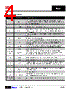
4 / 51 page  IR3447 4 www.irf.com © 2013 International Rectifier July 17, 2013 PIN DESCRIPTIONS PIN # PIN NAME PIN DESCRIPTION 1 PVin Input voltage for power stage. Bypass capacitors between PVin and PGND should be connected very close to this pin and PGND; also forms input to feedforward block 2 Boot Supply voltage for high side driver 3 Enable Enable pin to turning on and off the IC. 4 Rt/Sync Use an external resistor from this pin to LGND to set the switching frequency, very close to the pin. This pin can also be used for external synchronization. 5 OCset Current Limit setpoint. This pin allows the trip point to be set to one of three possible settings by either floating this pin, tying it to VCC or tying it to PGnd. 6 Vsns Sense pin for OVP and PGood 7 FB Inverting input to the error amplifier. This pin is connected directly to the output of the regulator or to the output of the remote sense amplifier, via resistor divider to set the output voltage and provide feedback to the error amplifier. 8 COMP Output of error amplifier. An external resistor and capacitor network is typically connected from this pin to FB to provide loop compensation. 9 RSo Remote Sense Amplifier Output 10, 26, 27, 29 PGND Power ground. This pin should be connected to the system’s power ground plane. Bypass capacitors between PVin and PGND should be connected very close to PVIN pin (pin 1) and this pin. 11 LGND Signal ground for internal reference and control circuitry. 12 RS- Remote Sense Amplifier input. Connect to ground at the load. 13 RS+ Remote Sense Amplifier input. Connect to output at the load. 14 CByp Bypassing capacitor for internal reference voltage. A capacitor between 100pF and 180pF should be connected between this pin and LGnd. 15, 19, 28, 30, 31, 33 NC No connection. 16 PGD Power Good status pin. Output is open drain. Connect a pull up resistor from this pin to VCC. 17 Vin Input Voltage for LDO. 18 VCC/LDO_out Bias Voltage for IC and driver section, output of LDO. Add a minimum of 4.7uF bypass cap from this pin to PGnd. 20, 21, 22, 23, 24, 25, 32 SW Switch node. This pin is connected to the output inductor. |
|
링크 URL |
| ALLDATASHEET 가 귀하에 도움이 되셨나요? [ DONATE ] |
Alldatasheet는? | 광고문의 | 운영자에게 연락하기 | 개인정보취급방침 | 링크 투 데이터시트 | 링크교환 | 제조사별 검색 All Rights Reserved©Alldatasheet.com |
| Russian : Alldatasheetru.com | Korean : Alldatasheet.co.kr | Spanish : Alldatasheet.es | French : Alldatasheet.fr | Italian : Alldatasheetit.com Portuguese : Alldatasheetpt.com | Polish : Alldatasheet.pl | Vietnamese : Alldatasheet.vn Indian : Alldatasheet.in | Mexican : Alldatasheet.com.mx | British : Alldatasheet.co.uk | New Zealand : Alldatasheet.co.nz |
|
Family Site : ic2ic.com |
icmetro.com |
 Korean ▼
 English
 Chinese
 German
 Japanese
 Russian
 Korean
 Spanish
 French
 Italian
 Portuguese
 Polish
 Vietnamese
 Indian
 Mexican
 British
 New Zealand