|
전자부품 데이터시트 검색엔진 |
|
|
전자부품 데이터시트 검색엔진 |
|
LTC3400 데이터시트(PDF) 4 Page - Linear Technology |
|
|
|||||||||||||||||||||||||||||
LTC3400 데이터시트(HTML) 4 Page - Linear Technology |
|
|
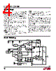
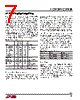
4 / 12 page  LTC3400/LTC3400B 4 3400fa PI FU CTIO S SW (Pin 1): Switch Pin. Connect inductor between SW and VIN. Optional Schottky diode is connected between SW and VOUT. Keep these PCB trace lengths as short and wide as possible to reduce EMI and voltage overshoot. If the inductor current falls to zero, or SHDN is low, an internal 100 Ω antiringing switch is connected from SW to VIN to minimize EMI. GND (Pin 2): Signal and Power Ground. Provide a short direct PCB path between GND and the (–) side of the output capacitor(s). FB (Pin 3): Feedback Input to the gm Error Amplifier. Connect resistor divider tap to this pin. The output voltage can be adjusted from 2.5V to 5V by: VOUT = 1.23V • [1 + (R1/R2)] SHDN (Pin 4): Logic Controlled Shutdown Input. SHDN = High: Normal free running operation, 1.2MHz typical operating frequency. SHDN = Low: Shutdown, quiescent current < 1 µA. 100 Ω connected between SW and VIN. Typically, SHDN should be connected to VIN through a 1M pull-up resistor. VOUT (Pin 5): Output Voltage Sense Input and Drain of the Internal Synchronous Rectifier MOSFET. Bias is derived from VOUT. PCB trace length from VOUT to the output filter capacitor(s) should be as short and wide as possible. VOUT is held at VIN – 0.6V in shutdown due to the body diode of the internal PMOS. VIN (Pin 6): Battery Input Voltage. The device gets its start-up bias from VIN. Once VOUT exceeds VIN, bias comes from VOUT. Thus, once started, operation is com- pletely independent from VIN. Operation is only limited by the output power level and the battery’s internal series resistance. 1.23V REF Burst Mode OPERATION CONTROL SHUTDOWN CONTROL SLOPE COMP PWM CONTROL START-UP OSC MUX A B A/B RAMP GEN 1.2MHz FB 3400 BD 3 VOUT OPTIONAL SCHOTTKY L1 4.7 µH 5 SW 1 VIN SINGLE CELL INPUT 6 SHDN 4 GND 2 gm ERROR AMP VOUT GOOD PWM COMPARATOR RC 80k SHUTDOWN CC 150pF CP2 2.5pF R2 604k 1% (EXTERNAL) R1 1.02M 1% (EXTERNAL) SLEEP Σ SYNC DRIVE CONTROL 0.35 Ω 0.45 Ω 2.3V COUT 4.7 µF 3.3V OUTPUT CIN 1 µF + CURRENT SENSE CFF (OPTIONAL) BLOCK DIAGRA |
|
|
링크 URL |
| ALLDATASHEET 가 귀하에 도움이 되셨나요? [ DONATE ] |
Alldatasheet는? | 광고문의 | 운영자에게 연락하기 | 개인정보취급방침 | 링크 투 데이터시트 | 링크교환 | 제조사별 검색 All Rights Reserved©Alldatasheet.com |
| Russian : Alldatasheetru.com | Korean : Alldatasheet.co.kr | Spanish : Alldatasheet.es | French : Alldatasheet.fr | Italian : Alldatasheetit.com Portuguese : Alldatasheetpt.com | Polish : Alldatasheet.pl | Vietnamese : Alldatasheet.vn Indian : Alldatasheet.in | Mexican : Alldatasheet.com.mx | British : Alldatasheet.co.uk | New Zealand : Alldatasheet.co.nz |
|
Family Site : ic2ic.com |
icmetro.com |
 Korean ▼
 English
 Chinese
 German
 Japanese
 Russian
 Korean
 Spanish
 French
 Italian
 Portuguese
 Polish
 Vietnamese
 Indian
 Mexican
 British
 New Zealand