|
전자부품 데이터시트 검색엔진 |
|
|
전자부품 데이터시트 검색엔진 |
|
ADP1611ARMZ-R7 데이터시트(PDF) 12 Page - Analog Devices |
|
|
|||||||||||||||||||||||||||||
ADP1611ARMZ-R7 데이터시트(HTML) 12 Page - Analog Devices |
|
|
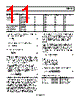
12 / 20 page  ADP1611 Rev. 0 | Page 12 of 20 DIODE SELECTION The output rectifier conducts the inductor current to the output capacitor and load while the switch is off. For high efficiency, minimize the forward voltage drop of the diode. For this reason, Schottky rectifiers are recommended. However, for high voltage, high temperature applications where the Schottky rectifier reverse leakage current becomes significant and can degrade efficiency, use an ultrafast junction diode. Make sure that the diode is rated to handle the average output load current. Many diode manufacturers derate the current capability of the diode as a function of the duty cycle. Verify that the output diode is rated to handle the average output load current with the minimum duty cycle. The minimum duty cycle of the ADP1611 is OUT MAX IN OUT MIN V V V D − − = (10) where VIN-MAX is the maximum input voltage. Table 6. Schottky Diode Manufacturers Vendor Phone No. Web Address On Semiconductor 602-244-6600 www.onsemi.com Diodes, Inc. 805-446-4800 www.diodes.com Central Semiconductor 631-435-1110 www.centralsemi.com Sanyo 310-322-3331 www.sanyo.com LOOP COMPENSATION The ADP1611 uses external components to compensate the regulator loop, allowing optimization of the loop dynamics for a given application. The step-up converter produces an undesirable right-half plane zero in the regulation feedback loop. This requires compen- sating the regulator such that the crossover frequency occurs well below the frequency of the right-half plane zero. The right- half plane zero is determined by the following equation: L R V V RHP F LOAD OUT IN Z × × ⎟⎟ ⎠ ⎞ ⎜⎜ ⎝ ⎛ = π 2 ) ( 2 (11) where: FZ(RHP) is the right-half plane zero. RLOAD is the equivalent load resistance or the output voltage divided by the load current. To stabilize the regulator, ensure that the regulator crossover frequency is less than or equal to one-fifth of the right-half plane zero and less than or equal to one-fifteenth of the switching frequency. The regulator loop gain is OUT CS COMP MEA OUT IN OUT FB VL Z G Z G V V V V A × × × × × = (12) where: AVL is the loop gain. VFB is the feedback regulation voltage, 1.230 V. VOUT is the regulated output voltage. VIN is the input voltage. GMEA is the error amplifier transconductance gain. ZCOMP is the impedance of the series RC network from COMP to GND. GCS is the current-sense transconductance gain (the inductor current divided by the voltage at COMP), which is internally set by the ADP1611. ZOUT is the impedance of the load and output capacitor. To determine the crossover frequency, it is important to note that, at that frequency, the compensation impedance (ZCOMP) is dominated by the resistor, and the output impedance (ZOUT) is dominated by the impedance of the output capacitor. So, when solving for the crossover frequency, the equation (by definition of the crossover frequency) is simplified to 1 2 1 | | = × × × × × × × = OUT C C f CS G COMP R MEA G OUT V IN V OUT V FB V VL A π (13) where fC is the crossover frequency and RCOMP is the compensation resistor. Solving for RCOMP CS MEA IN FB OUT OUT OUT C COMP G G V V V V C f R × × × × × × × = π 2 (14) For VFB = 1.23, GMEA = 100 µS, and GCS = 2 S IN OUT OUT OUT C COMP V V V C f R × × × × × = 4 10 55 . 2 (15) Once the compensation resistor is known, set the zero formed by the compensation capacitor and resistor to one-fourth of the crossover frequency, or COMP C COMP R f C × × = π 2 (16) where CCOMP is the compensation capacitor. The capacitor, C2, is chosen to cancel the zero introduced by output capacitance ESR. Solving for C2, COMP OUT R C ESR C2 × = (17) |
|
|
링크 URL |
| ALLDATASHEET 가 귀하에 도움이 되셨나요? [ DONATE ] |
Alldatasheet는? | 광고문의 | 운영자에게 연락하기 | 개인정보취급방침 | 링크 투 데이터시트 | 링크교환 | 제조사별 검색 All Rights Reserved©Alldatasheet.com |
| Russian : Alldatasheetru.com | Korean : Alldatasheet.co.kr | Spanish : Alldatasheet.es | French : Alldatasheet.fr | Italian : Alldatasheetit.com Portuguese : Alldatasheetpt.com | Polish : Alldatasheet.pl | Vietnamese : Alldatasheet.vn Indian : Alldatasheet.in | Mexican : Alldatasheet.com.mx | British : Alldatasheet.co.uk | New Zealand : Alldatasheet.co.nz |
|
Family Site : ic2ic.com |
icmetro.com |
 Korean ▼
 English
 Chinese
 German
 Japanese
 Russian
 Korean
 Spanish
 French
 Italian
 Portuguese
 Polish
 Vietnamese
 Indian
 Mexican
 British
 New Zealand