|
전자부품 데이터시트 검색엔진 |
|
|
전자부품 데이터시트 검색엔진 |
|
ADP1611ARMZ-R7 데이터시트(PDF) 15 Page - Analog Devices |
|
|
|||||||||||||||||||||||||||||
ADP1611ARMZ-R7 데이터시트(HTML) 15 Page - Analog Devices |
|
|
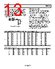
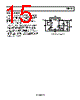
15 / 20 page  ADP1611 Rev. 0 | Page 15 of 20 SEPIC POWER SUPPLY The circuit in Figure 30 shows the ADP1611 in a single-ended primary inductance converter (SEPIC) topology. This topology is useful for an unregulated input voltage, such as a battery- powered application in which the input voltage can vary between 2.7 V to 5 V, and the regulated output voltage falls within the input voltage range. The input and the output are dc-isolated by a coupling capaci- tor, C1. In steady state, the average voltage of C1 is the input voltage. When the ADP1611 switch turns on and the diode turns off, the input voltage provides energy to L1, and C1 provides energy to L2. When the ADP1611 switch turns off and the diode turns on, the energy in L1 and L2 is released to charge the output capacitor, COUT, and the coupling capacitor, C1, and to supply current to the load. 2.5V–5.5V 3.3V IN SD SS RT SW ON FB COMP CSS 22nF GND L1 4.7 µH L2 4.7 µH ADP1611 5 6 3 2 7 8 1 4 CIN 10 µF CCOMP 1nF RCOMP 60k Ω COUT 10 µF C1 10 µF R1 16.8k Ω R2 10k Ω Figure 30. 3.3 V DC-to-DC Converter |
|
|
링크 URL |
| ALLDATASHEET 가 귀하에 도움이 되셨나요? [ DONATE ] |
Alldatasheet는? | 광고문의 | 운영자에게 연락하기 | 개인정보취급방침 | 링크 투 데이터시트 | 링크교환 | 제조사별 검색 All Rights Reserved©Alldatasheet.com |
| Russian : Alldatasheetru.com | Korean : Alldatasheet.co.kr | Spanish : Alldatasheet.es | French : Alldatasheet.fr | Italian : Alldatasheetit.com Portuguese : Alldatasheetpt.com | Polish : Alldatasheet.pl | Vietnamese : Alldatasheet.vn Indian : Alldatasheet.in | Mexican : Alldatasheet.com.mx | British : Alldatasheet.co.uk | New Zealand : Alldatasheet.co.nz |
|
Family Site : ic2ic.com |
icmetro.com |
 Korean ▼
 English
 Chinese
 German
 Japanese
 Russian
 Korean
 Spanish
 French
 Italian
 Portuguese
 Polish
 Vietnamese
 Indian
 Mexican
 British
 New Zealand