|
전자부품 데이터시트 검색엔진 |
|
|
전자부품 데이터시트 검색엔진 |
|
ADP1611ARMZ-R7 데이터시트(PDF) 14 Page - Analog Devices |
|
|
|||||||||||||||||||||||||||||
ADP1611ARMZ-R7 데이터시트(HTML) 14 Page - Analog Devices |
|
|
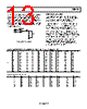
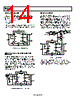
14 / 20 page  ADP1611 Rev. 0 | Page 14 of 20 APPLICATION CIRCUITS The circuit in Figure 27 shows the ADP1611 in a step-up configuration. The ADP1611 is used here to generate a 15 V regulator with the following specifications: VIN = 3.5 V to 5.5 V VOUT = 15 V IOUT ≤ 400 mA The output can be set to the desired voltage using Equation 2. Use Equations 16 and 17 to change the compensation network. IN SD SS RT SW ON FB COMP CSS 22nF GND L1 4.7 µH D1 ADP1611 5 6 3 2 7 8 1 4 CIN 10 µF CCOMP 150pF RCOMP 220k Ω COUT 10 µF R1 112k Ω R2 10k Ω 5V 15V Figure 27. 5 V to 15 V Step-Up Regulator STEP-UP DC-TO-DC CONVERTER WITH TRUE SHUTDOWN Some battery-powered applications require very low standby current. The ADP1611 typically consumes 10 nA from the input, which makes it suitable for these applications. However, the output is connected to the input through the inductor and the rectifying diode, allowing load current draw from the input while shut down. The circuit in Figure 28 enables the ADP1611 to achieve output load disconnect at shutdown. To shut down the ADP1611 and disconnect the output from the input, drive the SD pin below 0.4 V. IN SHDN SS RT SW FB COMP 22nF GND 4.7 µH ADP1611 5 6 3 2 7 8 1 4 10 µF B Q1 A Q1 FDC6331 150pF 220k Ω 10 µF 112k Ω ON 10k Ω 10k Ω 5V 15V Figure 28. Step-Up Regulator with True Shutdown TFT LCD BIAS SUPPLY Figure 29 shows a power supply circuit for TFT LCD module applications. This circuit has +10 V, −5 V, and +22 V outputs. The +10 V is generated in the step-up configuration. The −5 V and +22 V are generated by the charge-pump circuit. During step-up , the SW node switches between 10 V and ground (neglecting forward drop of the diode and on resistance of the switch). When the SW node is high, C5 charges up to 10 V. C5 holds its charge and forward-biases D8 to charge C6 to −10 V. The Zener diode, D9, clamps and regulates the output to −5 V. IN SD SS RT SW ON FB COMP CSS 22nF GND L1 4.7 µH D1 D2 D3 BAV99 BAV99 BZT52C22 BZT52C5VIS BAV99 ADP1611 5 6 3 2 7 8 1 4 C1 10nF CIN 10 µF CCOMP 150pF RCOMP 220k Ω COUT 10 µF C2 1 µF C3 10 µF R1 71.3k Ω R2 10k Ω D5 D9 3.3V VGL –5V VGH 22V 10V D5 D4 D8 D7 C4 10nF R3 200 Ω C5 10nF C6 10 µF R4 200 Ω Figure 29. TFT LCD Bias Supply The VGH output is generated in a similar manner by the charge-pump capacitors, C1, C2, and C4. The output voltage is tripled and regulated down to 22 V by the Zener diode, D5. |
|
|
링크 URL |
| ALLDATASHEET 가 귀하에 도움이 되셨나요? [ DONATE ] |
Alldatasheet는? | 광고문의 | 운영자에게 연락하기 | 개인정보취급방침 | 링크 투 데이터시트 | 링크교환 | 제조사별 검색 All Rights Reserved©Alldatasheet.com |
| Russian : Alldatasheetru.com | Korean : Alldatasheet.co.kr | Spanish : Alldatasheet.es | French : Alldatasheet.fr | Italian : Alldatasheetit.com Portuguese : Alldatasheetpt.com | Polish : Alldatasheet.pl | Vietnamese : Alldatasheet.vn Indian : Alldatasheet.in | Mexican : Alldatasheet.com.mx | British : Alldatasheet.co.uk | New Zealand : Alldatasheet.co.nz |
|
Family Site : ic2ic.com |
icmetro.com |
 Korean ▼
 English
 Chinese
 German
 Japanese
 Russian
 Korean
 Spanish
 French
 Italian
 Portuguese
 Polish
 Vietnamese
 Indian
 Mexican
 British
 New Zealand